



Content last revised on September 10, 2026
7MBR150XNA065-50 Operational Boundaries: Evaluating Baseplate Convexity Compensation and Screw Limits
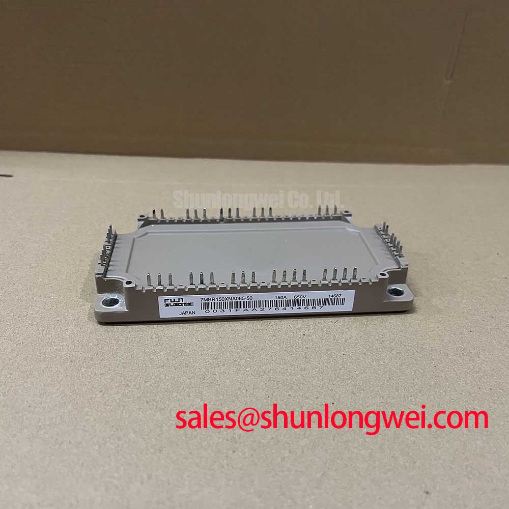
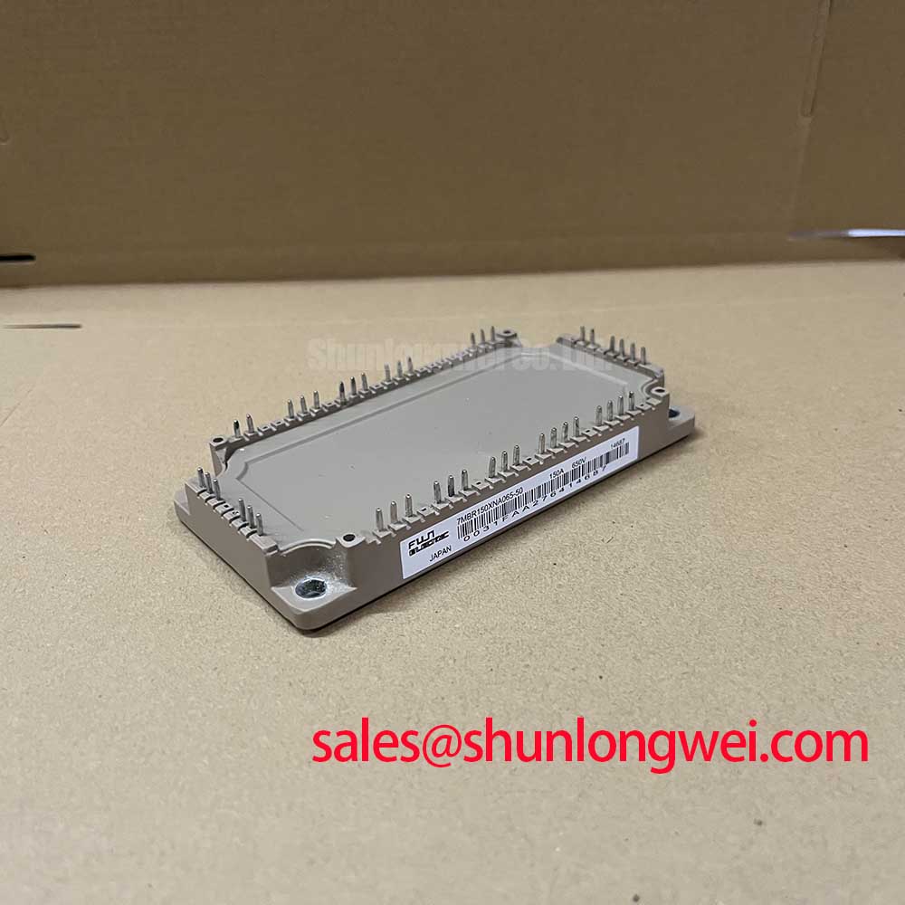
Before fitting 7MBR150XNA065-50, verify that the installed inverter assembly was designed around a 650 V collector emitter rating and a 150 A DC collector current at Tc = 100°C, then inspect the heatsink contact area for debris, raised burrs, corrosion, and old thermal compound.
The Fuji Electric 7MBR150XNA065-50 is specified with Vces = 650 V, Ic = 150 A at Tc = 100°C, and a maximum specified junction temperature of +175°C. These are Official Datasheet Specifications and define the electrical and thermal boundaries that maintenance teams should confirm before returning an inverter welder or medium frequency induction heating supply to service.
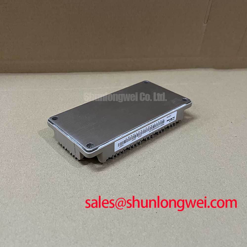
Heatsink flatness is a practical first concern because a clean module can still run hot when its baseplate does not make uniform contact with the cooling surface. As a Design Consideration, apply thermal interface material as a thin, continuous film in the approximate 50 to 100 μm range where the selected material and assembly process support that thickness. The objective is to fill microscopic surface irregularities without creating a thick thermal barrier. If the removed compound is dry, uneven, or visibly displaced toward one edge, inspect both the module baseplate and heatsink for distortion before reinstalling.
Baseplate curvature and heatsink unevenness should be assessed together. A straightedge inspection can reveal whether the mounting plane has been damaged by previous over tightening, contamination, or local impact. Do not attempt to compensate for a visibly uneven mounting surface by applying excessive thermal compound. That approach can hide a mechanical issue while increasing thermal resistance under load.
Mounting screws should be engaged gradually in a crosswise sequence so clamping pressure develops evenly. The final torque must follow the equipment manufacturer’s mechanical documentation and the relevant Fuji Electric package documentation rather than a generic shop value. This prevents local baseplate stress and helps maintain predictable thermal transfer.
⚠️ Maintenance Note: After reassembly, monitor heatsink contact temperature and confirm that the cooling airflow path is clean before applying sustained welding or induction heating load.
| Official Specification | Value | Service Relevance |
|---|---|---|
| Collector Emitter Voltage | 650 V | DC bus and transient verification boundary |
| Collector Current at Tc = 100°C | 150 A DC | Continuous current reference for thermal evaluation |
| Maximum Junction Temperature | +175°C | Upper semiconductor temperature limit |
| IGBT Junction to Case Thermal Resistance | 0.28 K/W maximum | Thermal path reference before interface resistance |
Assembly Integrity & Layout Architecture: Implementing Thermal Time Constants and Peak Junction for 7MBR150XNA065-50
For pulsed overload work, junction temperature cannot be judged from case temperature alone. The official maximum IGBT junction to case thermal resistance is 0.28 K/W, but the actual junction excursion during short welding pulses depends on transient thermal impedance, pulse width, pulse repetition, current waveform, cooling condition, and the thermal interface between module and heatsink.
A multi RC thermal model can estimate the changing thermal impedance during a pulse train, but a defensible calculation requires the manufacturer transient thermal impedance curves and the actual electrical loss profile. Those curves are not included in the supplied parameter set for this product page, so a numerical peak junction calculation should not be assumed here. As an Engineering Recommendation, technicians should compare measured case temperature trends, load duration, switching waveforms, and cooling performance against a known functional power stage before approving heavy pulsed operation.
The published switching-loss references are Eon = 15.0 mJ typical and Eoff = 15.0 mJ typical at Ic = 150 A. These values are Official Datasheet Specifications under the stated test condition, not fixed operating losses for every inverter. Switching loss changes with the implemented gate drive, current, DC bus voltage, junction temperature, snubber arrangement, and commutation path. The antiparallel diode is specified with VF = 1.75 V typical at IF = 150 A and Err = 11.0 mJ typical at IF = 150 A, both of which belong in a complete loss assessment.
Bootstrap supply integrity for a high side driver also requires information not provided here, including the selected driver quiescent current, gate charge, operating frequency, allowed bootstrap voltage droop, and refresh interval. A capacitor value should therefore be calculated from the complete driver circuit requirements, rather than inferred from the module current rating. If a high side command becomes inconsistent under duty changes, inspect the bootstrap recharge interval, local driver supply decoupling, and gate voltage at the driver reference point.
For current-related loss estimation, RMS current is usually more useful than a simple average-current assumption because heating follows the time-varying current waveform. The underlying RMS principle is described in this reference on Root Mean Square current calculations. In maintenance practice, the measured waveform must remain the governing input.
7MBR150XNA065-50 Thermal-Electrical Optimization: Differential Gate-Source Loop Routing to Practical Tuning
Gate-loop behavior should be checked at the installed assembly level rather than predicted from a current rating alone. During switching, voltage developed across shared power-return inductance can alter the effective gate emitter voltage seen by the IGBT. This may appear as waveform ringing, inconsistent switching edges, unwanted gate movement, or a gate drive protection response. Each observation needs oscilloscope confirmation against a known-good signal path because several assembly and control issues can produce similar symptoms.
As a Design Consideration, keep the gate drive loop physically compact and separate its return route from the main high-current emitter path wherever the package terminal arrangement supports that routing. The integrator should verify the exact terminal designations from the original module documentation before assuming the availability of a dedicated auxiliary emitter or Kelvin reference connection. A power module should never be rewired on the basis of a general package convention.
When evaluating a repaired inverter welder, capture gate emitter voltage and collector emitter voltage with measurement methods suited to the voltage and switching environment. Confirm dead-time behavior, turn-on overlap risk, and turn-off overshoot under controlled conditions. The system engineer should tune gate resistance and any snubber network only after verifying peak voltage margins against the actual DC-link voltage during switching tests.
The module’s listed conduction characteristics provide useful reference points: VCE(sat) = 1.70 V typical at Ic = 150 A and VCE(sat) = 1.75 V typical at Ic = 75 A. These are Official Datasheet Specifications, but live measurements can differ because of temperature, measurement placement, load waveform, and drive conditions. A rising conduction drop under otherwise comparable operation can justify checking gate drive amplitude, terminal contact condition, cooling, and load current before making a component-level diagnosis.
For a neutral comparison during repair planning, engineers may review the electrical and mechanical documentation for the 2MBI150UC-120. Any substitution assessment must verify voltage class, topology, terminal arrangement, drive requirements, thermal interface, protection thresholds, and the full equipment schematic. Similar current figures alone do not establish interchangeability.
7MBR150XNA065-50 Thermal-Electrical Optimization: DC-Bus Operating Voltage Headroom Derating Practical Tuning
The 650 V Vces rating is the primary official blocking-voltage boundary for this module. In an inverter welder or induction heating power supply, the observed collector emitter peak can be influenced by the DC bus, commutation inductance, switching speed, braking energy, snubber condition, and the physical position of DC-link capacitors. During troubleshooting, inspect braking resistor circuits and regenerative energy paths where fitted, because failure in those system sections can change bus-voltage behavior independently of the IGBT module.
The diode’s specified reverse-voltage rating is a separate datasheet parameter, but it must not be interpreted as permission to operate the IGBT collector emitter path above its stated 650 V rating. Engineers should verify each rating against the applicable circuit node and original topology.
At sites above 2000 m, altitude, cooling density, installation environment, and system voltage stress deserve a dedicated Design Consideration. Terrestrial neutron exposure and single-event burnout risk are high-reliability subjects that cannot be converted into a product-specific FIT figure from the supplied specifications. No specific SEB rate, failure probability, or voltage derating percentage should be assigned without an applicable manufacturer source and a documented system-level assessment. Practical evaluation should instead include measured bus voltage, switching overshoot, thermal behavior, enclosure conditions, and the protection response during representative operating loads.
For technicians comparing resonant and bridge-based power stages during induction-heating service, Resonant Topologies in Home Appliances provides topology context that can help identify which commutation stresses must be measured in the original circuit. Product-family information can also be reviewed through the Fuji Electric Power Semiconductors Portal while confirming the exact documentation used by the equipment integrator.