


Content last revised on February 2, 2026
1MBI200SA-120B-52 IGBT Module: Engineering Insights for High-Efficiency Power Conversion
An Engineering Overview of the 1MBI200SA-120B-52
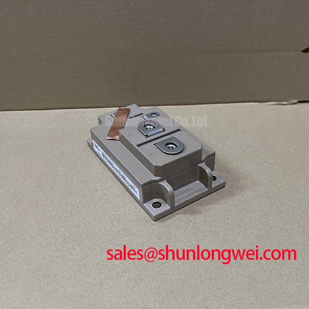
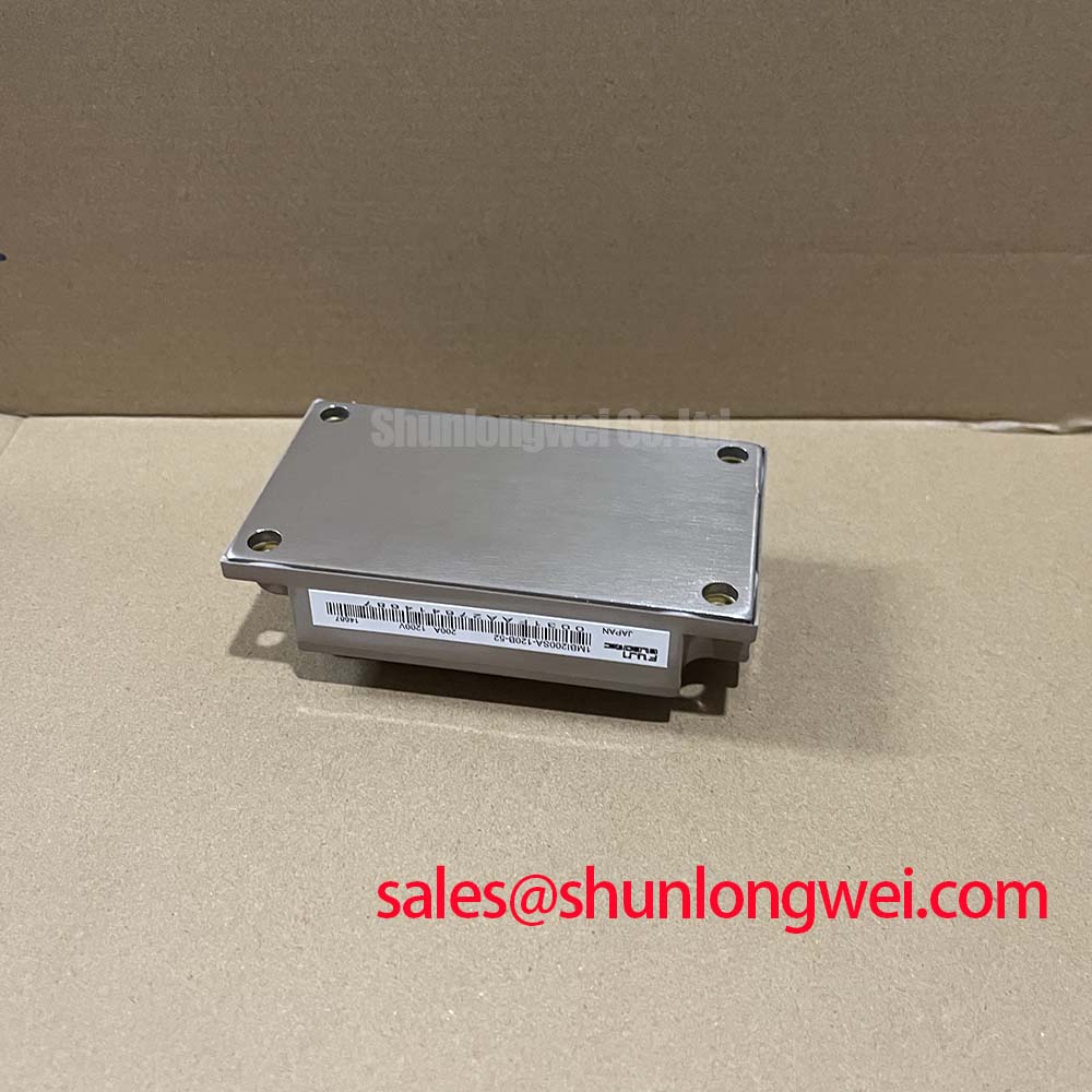
The Fuji Electric 1MBI200SA-120B-52 is a single-element IGBT module engineered for robust performance in high-power switching applications. It provides a strategic balance of low conduction losses and durable thermal performance, essential for demanding industrial environments. With key specifications of 1200V | 200A | VCE(sat) of 2.7V max, this device delivers high-current handling and superior efficiency. Its design prioritizes operational reliability and simplified thermal management. For systems requiring higher current capacity within the same voltage class, the related 1MBI300SA-120B offers an increased current rating. This module is an optimal choice for industrial drives and power converters where minimizing losses and ensuring stable operation are paramount design goals.
Application Scenarios & Value
Achieving System-Level Benefits in Industrial Motor Drives
The 1MBI200SA-120B-52 is engineered to excel in applications where efficiency and reliability are critical. Its primary use case is within the power stages of industrial systems such as Variable Frequency Drives (VFDs), servo drives, and general-purpose inverters. In a typical VFD application controlling a 75kW to 90kW AC motor, the IGBT's performance is central to system efficiency. The key engineering challenge is managing heat generated by switching and conduction losses, which directly impacts heatsink size, enclosure design, and long-term component life. The 1MBI200SA-120B-52 addresses this directly with its low collector-emitter saturation voltage (VCE(sat)) of 2.7V at its rated current. This parameter acts like a bottleneck for current flow; a lower value signifies less voltage drop and, consequently, lower power dissipated as heat during the 'on' state. This reduction in heat allows for more compact thermal solutions and enhances the overall power density of the inverter system.
Key Parameter Overview
Decoding the Specs for Efficient Power Switching
The technical specifications of the 1MBI200SA-120B-52 are foundational to its performance in power conversion systems. The table below highlights critical parameters and their direct engineering value.
| Parameter | Value | Engineering Value & Interpretation |
|---|---|---|
| Collector-Emitter Voltage (VCES) | 1200V | Provides a substantial safety margin for applications operating on 400V to 575V AC lines, ensuring reliability against voltage spikes. |
| Continuous Collector Current (IC) | 200A (at TC=80°C) | Enables control of high-power industrial motors and systems, offering significant current handling capability. |
| Collector-Emitter Saturation Voltage (VCE(sat)) | 2.7V (Max) | Directly translates to lower conduction losses. Think of it as the energy 'toll' for the current; a lower toll means less wasted energy (heat) and higher overall system efficiency. |
| Total Power Dissipation (PC) | 1130W | Defines the module's capacity to dissipate heat, a crucial factor for Thermal Management and determining operational limits. |
| Short Circuit Withstand Time (tsc) | 10µs | This is a critical reliability metric, indicating the module's robustness to survive a direct short-circuit condition for a brief period, allowing protective circuits to react. |
Industry Insights & Strategic Advantage
Meeting the Demands of Modern Industrial Automation
The drive for increased automation and energy efficiency in industrial settings places significant demands on power electronics. The 1MBI200SA-120B-52 aligns with these trends by enabling the design of more efficient and reliable power converters. Energy consumption standards for motor systems, such as those outlined by the IEC, push designers to minimize losses at every stage. A module with a low VCE(sat), like this one, is a key building block in achieving compliance and reducing the total cost of ownership for end-users through lower electricity consumption. Furthermore, as factories become more interconnected under the Industry 4.0 paradigm, the reliability of each component, including the central IGBT Module, becomes even more critical to prevent costly downtime.
Application Vignette
Enhancing Reliability in High-Cycle Servo Drive Systems
Consider a high-performance Servo Drive used in a robotic arm or CNC machine, applications characterized by rapid acceleration and deceleration cycles. This operational profile creates significant thermal stress on power modules. The 1MBI200SA-120B-52's robust thermal design and power dissipation capability (1130W) are crucial in this scenario. Its ability to efficiently transfer heat away from the IGBT chip to the heatsink ensures the junction temperature remains within its Safe Operating Area (SOA), even during peak load conditions. The effective management of this thermal load prevents premature component degradation, directly contributing to a longer service life and higher mean time between failures (MTBF) for the entire servo drive system, a critical metric for industrial machinery.
Frequently Asked Questions (FAQ)
What is the primary benefit of the 2.7V maximum VCE(sat) rating?
The low VCE(sat) directly reduces power loss during conduction. This means less heat is generated for the same amount of current, which can lead to smaller heatsink requirements, higher system efficiency, and improved operational reliability.
Is the 1MBI200SA-120B-52 suitable for hard-switching topologies?
Yes, its specifications are well-suited for standard hard-switching applications like those found in most industrial VFDs and power supplies. The datasheet provides detailed switching characteristics (Eon, Eoff) necessary for calculating losses in these designs.
How does the 1200V VCES rating translate to application voltage?
A 1200V rating provides the necessary design margin for robust operation on three-phase 400V, 480V, and even 575V AC industrial power grids, protecting the device from transient overvoltages common in such environments.
What does the 10µs short-circuit withstand time imply for system design?
It signifies a high level of ruggedness. This 10-microsecond window is critical for the gate drive and control circuitry to detect a fault condition and safely shut down the IGBT, preventing catastrophic failure of the module and the wider system.
What are the key considerations for the gate drive circuit for this module?
For optimal performance and to avoid parasitic turn-on, a gate drive capable of providing a clean +15V turn-on voltage and a negative turn-off voltage (e.g., -5V to -15V) is recommended. Proper gate resistance selection is also crucial to manage switching speed and EMI, as detailed in the official Fuji Electric application notes.
Design & Integration Support
An Engineer's Perspective on Implementation
When integrating the 1MBI200SA-120B-52, engineers should focus on three key areas for optimal results. First, a low-inductance laminated bus bar design is crucial to minimize voltage overshoot during high-speed switching events. Second, the gate drive layout should be meticulously planned, with short, direct traces to the module's gate and emitter terminals to ensure clean switching signals and prevent oscillation. Finally, ensuring a uniform and low-resistance thermal interface between the module's baseplate and the heatsink is paramount for maximizing heat extraction and long-term reliability. Proper mounting torque and the use of a high-quality thermal interface material are non-negotiable for leveraging the module's full thermal performance.