Temperature control is one of the key factors for the effective operation of MOSFET or IGBT module. Although some MOSFETs are equipped with an internal temperature sensor (body diode), other methods can also be used to monitor temperature. The semiconductor silicon PTC thermistor can perform current control well, or the platinum-based or niobium-based (RTD) resistance temperature detector can use a lower resistance to achieve higher detection linearity. Regardless of whether the sensor uses surface mount devices, wire-bonded die or sintered die, NTC thermistor is still a temperature sensor with excellent sensitivity and a wide range of applications. Proper design can ensure that the module is properly derated and eventually shut down the module in the event of overheating or high external temperature.

This article focuses on bonding NTC bare chips, and uses analog circuit simulation to illustrate the basic principles of power module derating and shutdown. Why simulation? Simulation is an ideal way to simplify and visually illustrate different phenomena, and is also suitable for developing intuitive applications. The last motivation is economic: we only use free software (LTspice) to develop simulations, while other design tools are used for more complex designs.
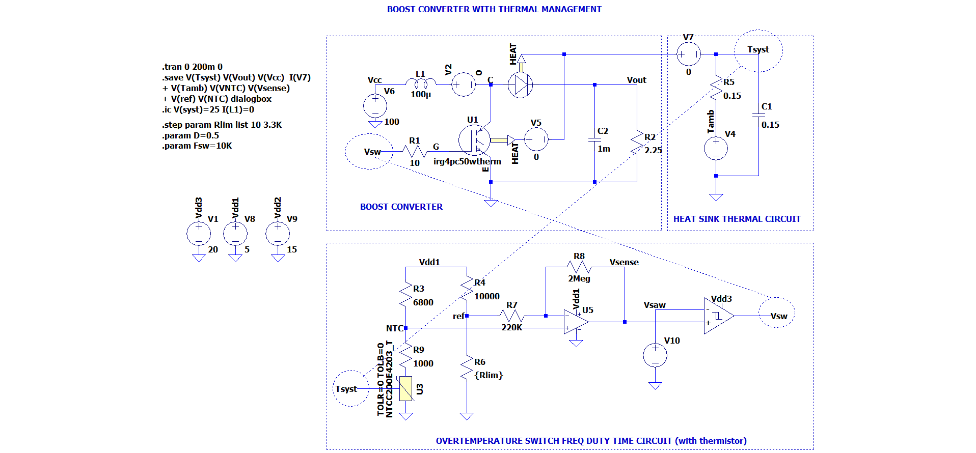
Now, let's look at the LTspice design shown in Figure 1, which is a simple boost converter design. However, due to the versatility of LTspice, the IGBT and diode models are replaced by thermal models, and the heat flux is clearly indicated by the output pin, which can be connected to a thermal circuit (such as a heat sink). We use a simple RC circuit (in reality, designers need to carefully define the Zth model as a Cauer or Foster model).
During the operation of the converter, the heat flux forms a hot spot (in this example, the node Tsyst generates a voltage and needs to control the temperature). This temperature is input to the NTC model (Vishay wire bond die NTCC200E4203_T). The NTC signal is compared with the threshold through the Wheatstone bridge, amplified, and compared with the sawtooth signal (Vsaw). The final output Vsw is a pulse signal applied to the gate of the IGBT. The Rlim resistance defines below the temperature threshold, and we apply a 100% full duty cycle pulse to the IGBT gate. When overheating—the IGBT and diode generate heat—plus the ambient temperature (thermal circuit node Tamb voltage), the duty cycle decreases, and the buck converter output/input ratio (Vout / Vcc) decreases. As a result, the heat decreases and the temperature begins to stabilize. Above a certain temperature limit, this ratio must be reduced to 1.
In order to complete the simulation in a reasonable time, the heat sink must be reduced. It may take several minutes or even hours for the heat increase, and we hope to see the effect within a short period of time.
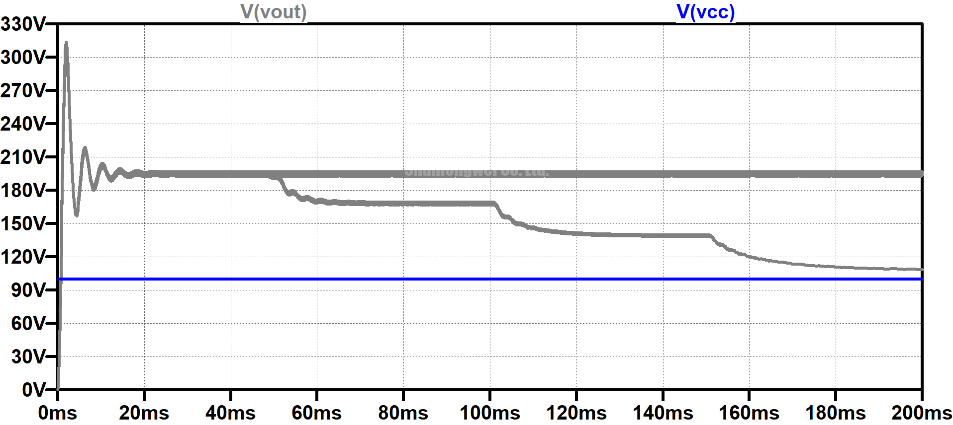
The following are the simulation results: the results shown in each figure with or without temperature derating (to cancel the temperature control, the value of Rlim is very low).
The boost converter usually oscillates in the first 20 ms, which is not optimized. The temperature Tsyst starts to rise, and then the ambient temperature rises. When Tsyst reaches 90 °C, Vout / Vcc starts to derate. Every time the ambient temperature rises a little, the duty cycle drops a little until the boost converter completely fails. At 110 °C, the derating reaches its maximum value.
Without temperature protection, Tsyst can reach 160 °C to 170 °C. In the actual power module, the peak temperature of the die can reach 200 °C or higher.
The voltages Vsense, Vntc and Vlim are shown in Figure 3. Figures 5 and 6 show the duty cycle changes at different times.
Of course, all thresholds are adjustable, and the switching thresholds can be adjusted accordingly.
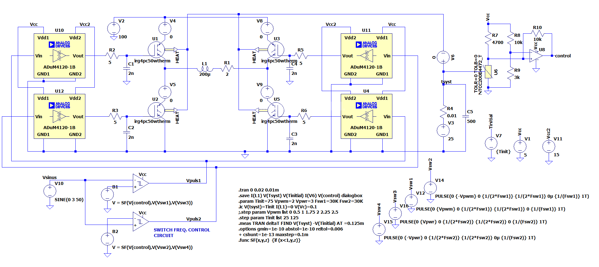
For more complex simulations, we can also rebuild the full-bridge IGBT module . The inductive load of this circuit generates a 50 Hz sinusoidal current and the IGBT switching frequency is 30 kHz. The gate driver simulation circuit maintains a constant frequency below 125 °C and reduces the duty cycle to reduce the loss of the IGBT above this temperature.
we can see the total thermal power generated by the IGBT switch (in W for I(V6)), and the temperature increase over time (in Celsius for V(Tsyst)).