Content last revised on September 10, 2026
Thermal Paste Degradation Prevention and Mechanical Clamping Torque Calibration
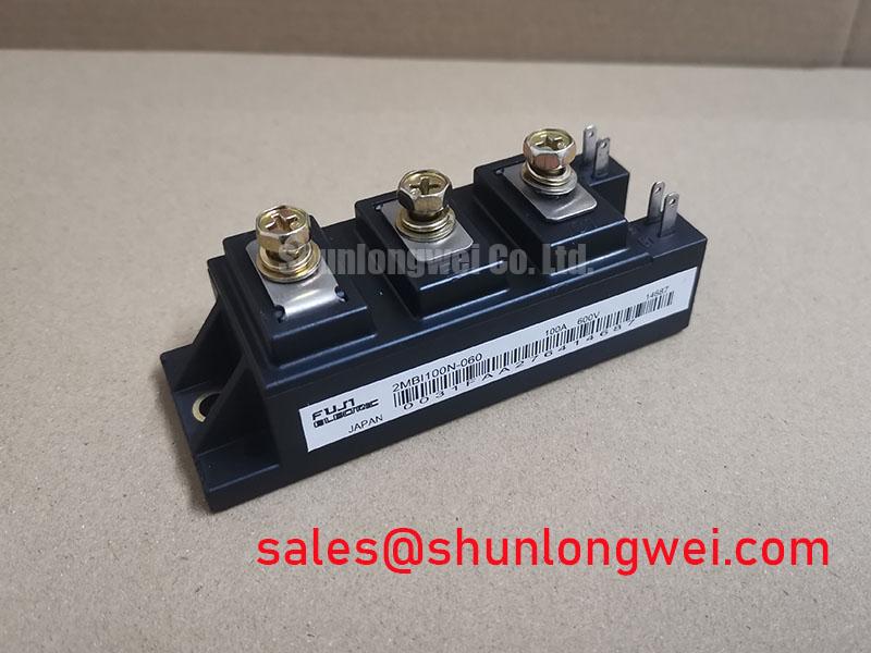
In commercial string inverters and micro-grid energy storage power conversion systems (PCS), thermal cycling presents the primary stress mechanism for dual power switches. The 2MBI100VA-060-50 dual IGBT module from Fuji Electric is rated for a continuous collector current of Ic = 100 A at Tc = 80°C and a total power dissipation of Pc = 480 W per IGBT switch at Tc = 25°C (Official Datasheet Specification). Maintaining junction temperatures within the rated Tj(max) = +150 °C envelope requires strict management of the thermal interface material (TIM) layer to preserve its low junction-to-case thermal resistance of Rth(j-c) = 0.26 °C/W for the IGBT and 0.45 °C/W for the freewheeling diode (FWD).
Baseplate warpage and void formation during high-temperature operation accelerate thermal degradation via Thermal Expansion Coefficient (CTE) Mismatch in Semiconductor Assemblies. Apply non-silicone or advanced phase-change TIM via screen printing at a wet thickness between 50 µm and 100 µm (Design Consideration). During heat sink mounting, apply a preliminary seating torque of 0.5 N·m across all mounting points before finalizing to the nominal fastening torque of 2.5 to 3.5 N·m (Design Consideration for standard M5 hardware).
⚠️ Field Alert: Never torque one mounting screw to maximum tension immediately. Uneven mechanical clamping creates asymmetrical internal baseplate bow, fracturing internal ceramic DCB substrates or pumping thermal grease out from beneath the high-heat IGBT dies, resulting in localized hot spots and rapid thermal runaway.
Kelvin Emitter Connection & Parasitic Inductance Minimization in High-Speed Switching
Operating high-frequency string inverters requires tight gate loop impedance control. Fast collector current transitions across parasitic trace inductances induce significant reverse voltages back into the gate loop if the drive return shares copper with the main power emitter. The 2MBI100VA-060-50 utilizes dedicated auxiliary emitter terminals (Kelvin emitter) to isolate gate control signals from the high di/dt power path.
To suppress Miller-effect turn-on caused by rapid switch node dV/dt displacement current charging Cres, route gate and Kelvin emitter tracks as tightly coupled twisted pairs or closely stacked PCB layers. Implementing an active Miller clamp or setting a negative turn-off bias (typically -5 V to -8 V, Design Consideration) stabilizes the gate below the threshold voltage during rapid commutation of the opposing switch. When servicing related high-power bridge assemblies, engineers managing higher DC-link stages frequently integrate topologies alongside complementary modules like the 2MBI200VH-120-50 for auxiliary booster or front-end converter stages.
Advanced planar architectures, such as those analyzed across Fuji Electric 7th-Gen X-Series IGBT Modules, demonstrate that minimizing loop inductance reduces diode reverse recovery snappy oscillations. Install high-frequency snubber film capacitors directly across the module's DC bus terminals (P and N) with lead lengths kept under 10 mm to clamp inductive overvoltage spikes during hard turn-off transitions.
High-Speed Fault Management: V_CE(sat) Desaturation Sensing Circuitry
Under short-circuit conditions in commercial inverters, fault current must be interrupted within the module's short-circuit safe operating area (SCSOA < 10 µs). The 2MBI100VA-060-50 exhibits a typical collector-emitter saturation voltage of VCE(sat) = 1.70 V (2.20 V max) at Ic = 100 A and Vge = 15 V (Official Datasheet Specification). Desaturation (DESAT) sensing circuits continuously monitor this forward drop during conduction.
When the collector-emitter voltage climbs above the preset DESAT threshold (typically 6.5 V to 7.5 V, Design Consideration) after the blanking time window (1.5 µs to 2.5 µs, Typical Starting Point), the driver must initiate a soft turn-off (SSD). Abruptly cutting off a saturated short-circuit current exceeding several hundred amperes generates catastrophic overshoots exceeding the VCES = 600 V breakdown rating.
For systems scaling to higher power densities within centralized sub-arrays, field engineers evaluating higher continuous current capacities can assess the pin-compatible higher-current variant 2MBI400VB-060-50. Detailed bench test methodology and diagnostic procedures for verifying gate drive desaturation timings are documented in the Field Engineer’s Handbook.
Cosmic Ray Robustness: Voltage Derating Curves across 2000m-4000m Altitudes
Utility and commercial micro-grid energy storage installations at high altitudes (2000 m to 4000 m above sea level) face accelerated terrestrial neutron flux, increasing the risk of Single Event Burnout (SEB). Because cosmic ray-induced failure rates rise exponentially with elevated DC bus voltages, modules rated at VCES = 600 V require conservative bus voltage derating at high altitudes.
| Parameter | Symbol | Official Datasheet Value | Test Conditions |
|---|---|---|---|
| Collector-Emitter Breakdown Voltage | VCES | 600 V | Tj = 25 °C |
| Continuous DC Collector Current | IC | 100 A | Tc = 80 °C |
| Collector-Emitter Saturation Voltage | VCE(sat) | 1.70 V (Typ) / 2.20 V (Max) | Ic = 100 A, Vge = 15 V, Tj = 25 °C |
| Forward Voltage (FWD) | VF | 1.70 V (Typ) / 2.20 V (Max) | If = 100 A, Vge = 0 V, Tj = 25 °C |
| Maximum Power Dissipation | Pc | 480 W | 1 Switch, Tc = 25 °C |
| Thermal Resistance (Junction-to-Case) | Rth(j-c) | 0.26 °C/W (IGBT) / 0.45 °C/W (FWD) | Per Device Base |
| Maximum Operating Temperature | Tj | +150 °C | Continuous Operation |
For installations operating above 2000 meters, limiting continuous DC bus operational levels to 380 V–420 V (Design Consideration based on standard terrestrial neutron derating models) ensures adequate safety margins against catastrophic latch-up while keeping junction thermal rise within strict design limits.