



Content last revised on September 22, 2026
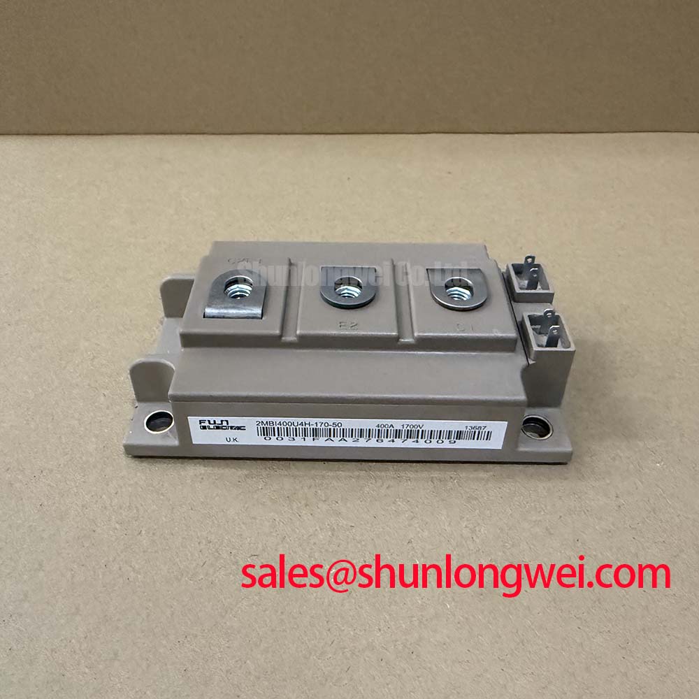
Field Diagnostics & Commissioning: Optimizing Heatsink Contact Pressure in 2MBI400U4H-170-50 Topologies
| Parameter | Official Specification |
|---|---|
| Manufacturer | Fuji Electric |
| Maximum collector-emitter voltage | 1700 V |
| Continuous collector current | 400 A at Tc = 80 °C |
| Total switching loss, typical | 160 mJ at Tj = 125 °C |
| Junction-to-case thermal resistance per IGBT | 0.086 °C/W |
| Maximum junction temperature | 150 °C |
| Short-circuit withstand time | 10 µs |
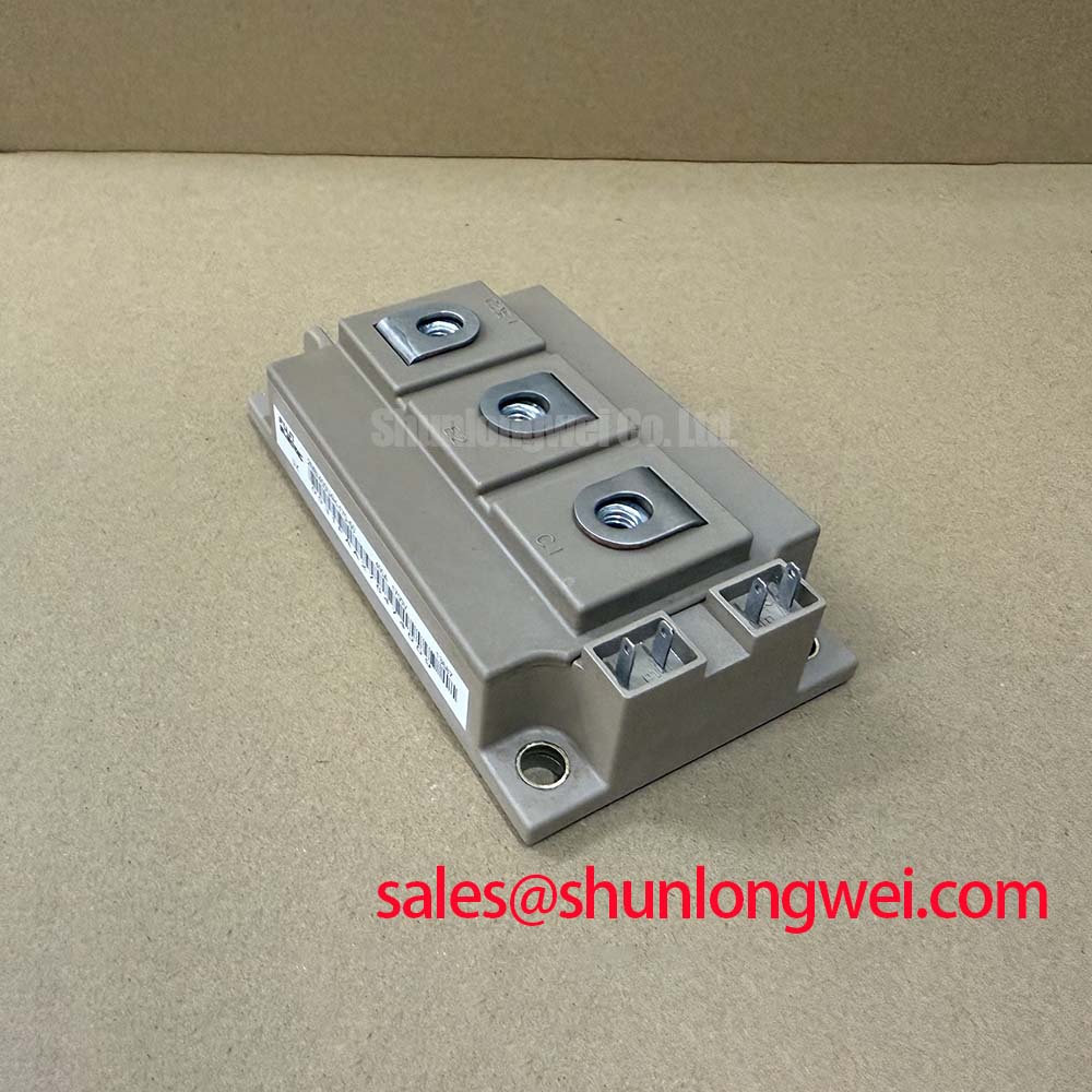
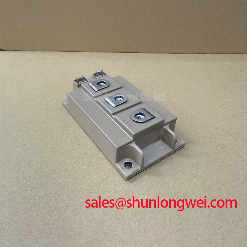
Thermal commissioning should begin with the mechanical interface rather than the gate-drive waveform. Clean the module contact area and heatsink with a suitable lint-free process, then inspect for burrs, embedded particles, surface damage, or visible curvature. Where the installation uses a baseplate and thermal interface material, the material should form a continuous, controlled layer without dry zones or trapped air. The frequently quoted 50–100 µm application range is a general assembly consideration, not an official parameter of this module; the correct thickness depends on the selected interface material, surface finish, mounting pressure, and supplier instructions.
Use the module manufacturer’s mechanical drawing and the selected heatsink documentation to establish the permitted flatness and contact conditions. A bowed mounting surface can create concentrated pressure near the fasteners while leaving insufficient contact elsewhere. This may produce an uneven temperature distribution even when the outer case feels secure. When a fixture uses a compliant plate or spring-loaded hardware, calibrate the applied load with the assembly supplier’s method rather than estimating pressure from screw rotation alone.
Sequential tightening should bring the module into contact progressively and evenly. A cross-pattern sequence is a common Design Consideration for reducing local distortion, but the final torque, washer arrangement, and fastening order must come from the applicable mechanical documentation. After installation, inspect the interface for displacement and confirm that the heatsink remains mechanically stable. Thermal measurements should be taken under a repeatable load, with attention to the case temperature near each active section rather than relying on a single remote heatsink reading.
The official Rth(j-c) value of 0.086 °C/W per IGBT is a component specification, not a complete system thermal resistance. Designers should combine it with the thermal interface, heatsink, airflow, coolant, ambient temperature, and switching-loss conditions. The listed 160 mJ typical total switching loss at Tj = 125 °C also requires interpretation against the real gate resistance, current, voltage, commutation path, and operating temperature. A thermal imbalance should therefore be investigated through contact inspection, current sharing checks, infrared or thermocouple measurements, and switching waveform review.
Field Diagnostics & Commissioning: High dv/dt Cross-Conduction Shoot-Through in 2MBI400U4H-170-50 Topologies
When commissioning a complementary IGBT leg, examine both gate-to-emitter waveforms and the collector-emitter transition with probes that have an appropriate bandwidth, insulation arrangement, and connection method. A high dv/dt transition can couple through parasitic capacitances and disturb the opposing gate circuit. The resulting waveform may show an unexpected gate excursion, delayed turn-off, or a brief overlap between the upper and lower switching devices. These observations do not prove a single failure mechanism; they indicate that the gate-drive loop, reference connection, timing, and measurement setup require coordinated review.
A dedicated low-impedance gate-return path is a useful Design Consideration, particularly where the power commutation loop carries high di/dt. An active Miller clamp may help hold the inactive gate near its intended off-state potential, but its suitability depends on the driver architecture and the module terminal arrangement. A negative gate bias is sometimes evaluated in high-noise converters, including values such as −5 V to −15 V in broader industry practice. Those values are not an official operating requirement stated here, so the system integrator must verify the allowable gate-emitter range from the relevant Fuji Electric documentation before applying them.
Dead-time should be established from measured turn-off delay, driver propagation variation, temperature, and the switching behavior of the complete leg. The objective is to prevent simultaneous conduction while avoiding excessive diode conduction or uncontrolled commutation. Treat dead-time as a system-determined timing parameter, then validate it through double-pulse testing and controlled load testing. The 10 µs short-circuit withstand time is an official module specification, but it should not be treated as a permission to delay protection; desaturation detection, soft shutdown, fault latching, and driver interlock behavior must be verified as a complete protection chain.
For traction inverter evaluation, inspect the isolated driver supply, common-mode transient immunity, desaturation blanking behavior, and fault propagation path. A driver that operates correctly on a low-voltage bench may behave differently when the power stage produces large common-mode transitions. The external reference on Fuji Electric’s Fuji Electric High-Speed Discrete IGBTs page can provide broader semiconductor context, but the final gate-voltage and protection limits must be confirmed against the documentation applicable to this module.
Assembly Integrity & Layout Architecture: Addressing Reflected-Wave Voltage Doubling in 2MBI400U4H-170-50 Systems
Long motor leads and discontinuities between the inverter output, cable, and motor can create reflected-wave behavior. A measured terminal spike approaching twice the applied voltage step is a system phenomenon associated with transmission-line effects and impedance mismatch; it is not an additional voltage rating of the IGBT module. The 1700 V maximum collector-emitter voltage must be compared with the measured peak at the module terminals under the fastest relevant switching condition, including temperature and load variation.
Begin the investigation at the module terminals. Use a properly rated differential probe with the shortest practical connection, then compare the waveform at the switching node, cable entry, and motor terminals. If the apparent overshoot changes substantially with probe placement, measurement inductance may be contributing to the observation. If the overshoot remains, designers should examine cable length, termination behavior, common-mode paths, and the physical arrangement of the DC-link and phase conductors.
Output reactors, dv/dt filters, ferrite structures, or other motor-side measures may reduce reflected-wave stress, but their selection is determined by motor insulation limits, cable characteristics, switching frequency, current, acoustic requirements, and thermal performance. Do not select a choke from the module current rating alone. Verify filter resonance, voltage drop, fault behavior, and control-loop interaction through system testing. The same principle applies to DC-link snubbers: their parasitic inductance, pulse energy, mounting position, and thermal dissipation must be evaluated at the actual switching node.
Clearance and creepage should be assessed from the working voltage, pollution environment, insulation system, altitude, material group, and applicable equipment standard. The module’s 1700 V rating does not independently establish a safe board or busbar spacing. High-voltage terminals should be routed to avoid unnecessary electric-field concentration, and sharp conductor edges should be controlled according to the insulation design. Where this part is evaluated for a high-speed rail or heavy freight locomotive traction inverter, the integrator should also verify vibration, contamination, cooling, and insulation coordination requirements for the complete converter.
Topology selection affects the stress seen by the switching devices. Engineers comparing quasi-resonant and half-bridge arrangements can consult Resonant Topologies in Home Appliances as a topology reference, while keeping the device voltage margin and switching test results specific to the actual inverter.
Preventing Spurious Faults: Optimizing Gate Drive Loop Geometry in 2MBI400U4H-170-50 Systems
Separate the gate-drive return from the high-current power return wherever the module’s terminal configuration permits. Mutual emitter coupling can introduce a voltage error into the driver reference during collector-current transitions, causing apparent gate oscillation, uneven turn-on, or nuisance protection trips. The practical objective is to minimize shared impedance in the gate loop and keep the outgoing gate path physically close to its return path.
Keep the driver, gate resistor network, isolation interface, and module connection arranged as a compact switching loop. Avoid routing sensitive gate traces alongside high-current collector or emitter conductors for long distances. If an auxiliary emitter or dedicated low-current reference terminal is provided in the applicable module drawing, use it only according to that documented function; do not assume that every external terminal has Kelvin behavior without confirmation.
Gate resistors, ferrite elements, active Miller clamps, and local decoupling should be selected after observing the real gate waveform. A resistor change can alter switching loss, overshoot, electromagnetic interference, and short-circuit response at the same time. The system engineer should verify the tradeoff using double-pulse tests, fault tests, and thermal measurements rather than selecting a value from a generic application circuit.
💡 Pro Tip: Keep the power commutation loop and gate-drive loop physically separated, then verify peak voltage, gate stability, and protection timing with isolated probes before connecting the full traction load.
For procurement or replacement evaluation, the 2MBI300U4H-120-50 may be reviewed as a separate Fuji Electric product for application comparison, but its voltage, current, thermal, and switching characteristics must be assessed independently rather than assumed interchangeable with the 2MBI400U4H-170-50.