



Content last revised on September 10, 2026
7MBR150U2R060-50 Thermal-Electrical Optimization: Managing High-C-Rate Battery Cycling Swing Practical Tuning
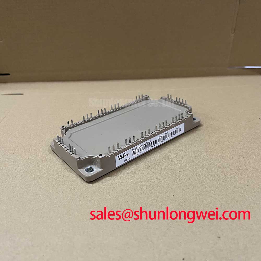
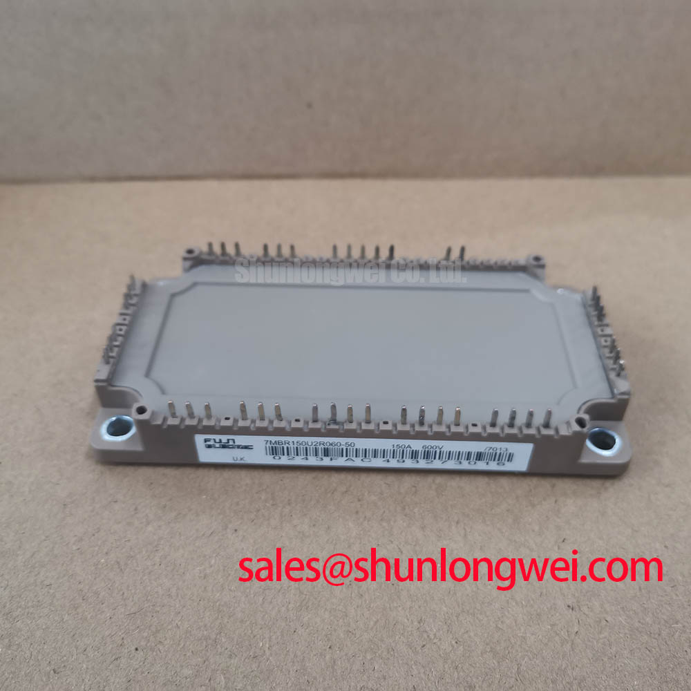
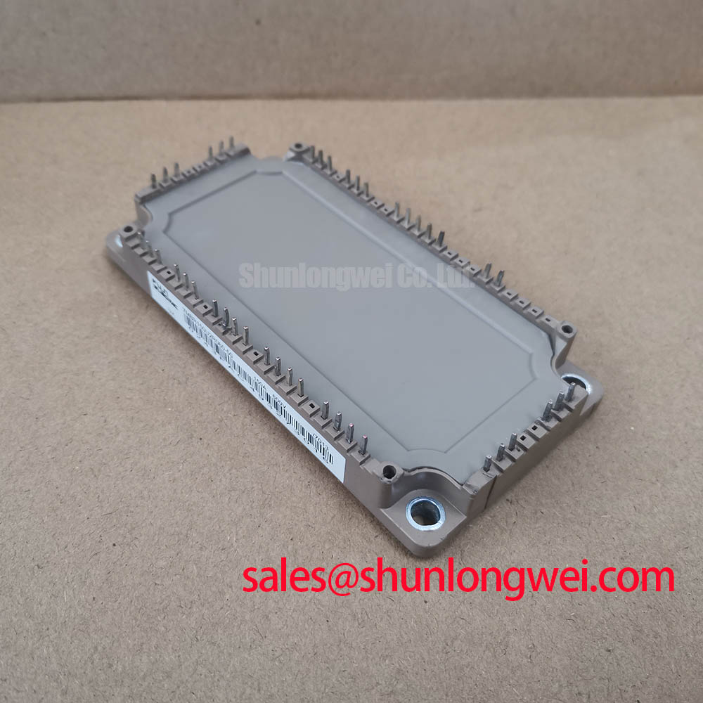
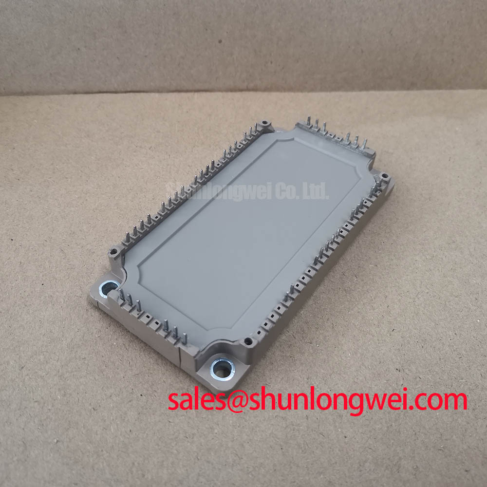
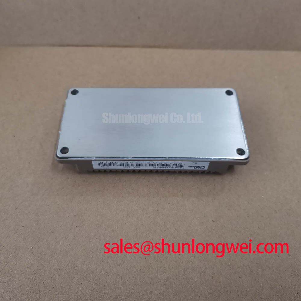
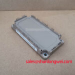
Begin incoming inspection by checking the 7MBR150U2R060-50 marking, module body, terminal condition, and rated electrical boundary before applying any test voltage. This Fuji Electric power module is specified at 600.0 V and 150.0 A, with a Module package classification. These are Official Specification values for identification and system evaluation; terminal layouts, switching characteristics, protection functions, and thermal limits should be confirmed against the applicable manufacturer documentation.
| Parameter | Official Specification |
|---|---|
| Manufacturer | Fuji Electric |
| Part number | 7MBR150U2R060-50 |
| Rated voltage | 600.0 V specified rating |
| Rated current | 150.0 A specified rating |
| Package | Module |
| Product category | PIM (Power Integrated Module) |
💡 Bench Tip: Use ESD protection, keep the device unpowered and discharged, and compare cold-state measurements with a known-good reference before connecting control or power wiring.
For a commercial string inverter or microgrid energy-storage converter, the module may be evaluated in a bidirectional power path between a battery rack and the inverter DC link. During charge and discharge transitions, the relevant engineering task is to correlate switching waveforms, phase-current sharing, heatsink temperature, and control timing rather than treating a temperature rise as proof of a single component fault.
Gate-loop routing should be short, physically separated from high-current commutation paths, and checked for unwanted coupling. Gate resistance, driver strength, dead time, and turn-off behavior are system-dependent Design Considerations. Engineers should tune them while observing gate-emitter voltage and collector-emitter transients on an oscilloscope. Any ringing should be evaluated against the confirmed module limits and the complete inverter topology.
When several semiconductor paths operate in parallel, positive temperature coefficient behavior can support static current sharing, but dynamic sharing still depends on gate-loop symmetry, conductor impedance, driver matching, and switching timing. Inspect busbar joints, terminal torque records, thermal interface coverage, and phase-current balance under controlled load changes. A replacement evaluation can include the related 7MBR20UF060 as a separately verified device, but substitution requires electrical, mechanical, gate-drive, and protection compatibility checks.
Benchtop Waveform Tuning: Mitigating Stress via DC-Bus Operating Voltage Headroom Derating on 7MBR150U2R060-50
The 600.0 V rating is an Official Specification, not a complete operating prescription for every DC-bus condition. Designers should establish voltage headroom from measured overshoot, switching frequency, temperature, load profile, and the inverter’s protection strategy. At elevated installation sites, cooling performance and insulation coordination may require site-specific review. No FIT rate or altitude derating value should be assigned without such a source.
For bench work, record the cold resistance and diode-test behavior only after identifying the correct terminals from the relevant documentation. A diode-test reading can help detect an unexpected open or short path, but the result is not a substitute for dynamic qualification. The system integrator should verify isolation requirements, creepage, clearance, and withstand-test conditions from the module documentation and applicable equipment standard.
Thermal interface material selection and mounting uniformity are Design Considerations. A thin, continuous TIM layer and a cross-pattern tightening sequence can reduce local thermal resistance and mechanical stress, but the suitable material, thickness, fastener method, and torque must be determined from the heatsink and manufacturer instructions. Verify the assembled thermal response during the intended load cycle rather than relying on visual inspection alone.
Transient Dynamics & Electrical Design: DC-Link Capacitance Bank Layout and Low-ES on 7MBR150U2R060-50
During turn-off, stray inductance and current slew rate can create collector-emitter overshoot. The relationship can be assessed in engineering calculations by treating the peak voltage as the DC-link voltage plus the inductive contribution from the commutation loop. This makes the physical arrangement of the DC-link capacitor bank, module terminals, and busbars a primary Design Consideration.
Use a compact, symmetrical laminated or planar bus structure where practical, minimize the high-current loop area, and keep capacitor connections close to the switching terminals. Snubber selection should be based on measured ringing frequency, energy, pulse repetition, capacitor voltage rating, and resistor pulse capability. MOVs can provide a complementary overvoltage absorption path, but their clamping behavior and energy rating must be coordinated with the DC-link protection network.
If the waveform shows unexpected spikes, compare measurements at the module terminals and at the capacitor bank, then check probe grounding, busbar joints, capacitor ESR, and gate timing. Designers should verify peak voltage margins during switching tests under the actual load and temperature range. The associated 7MBR50LC060 may be relevant to the upstream rectification topology, but it is not an automatic substitute for this module.
Preventing Spurious Faults: Isolated DC-DC Power Supply Sizing for 7MBR150U2R060-50
An isolated gate-drive supply should be evaluated as part of the complete switching system. Confirm the required gate voltage, supply current, startup sequence, fault-state behavior, isolation barrier, and common-mode transient performance from the driver and module documentation. Reinforced isolation and high CMTI figures are system-level requirements; they must not be assumed from the power-module part number alone.
Route isolated supply returns and gate-drive paths to control the intended reference potential, while keeping them away from high di/dt power conductors. Check the driver output with differential probing during turn-on, turn-off, battery charge, regenerative operation, and fault interruption. Spurious pulses may result from coupling, inadequate decoupling, reference movement, incorrect dead time, or measurement technique, so diagnosis should compare all gate channels against a known-good signal path.
Fuji Electric’s Power Semiconductor and IPM Modules information and its PIM 7-Pack reference provide useful manufacturer context for module-family evaluation. For broader topology review, engineers can consult Industrial Applications while validating the final design with measured electrical and thermal data.