

Content last revised on November 5, 2026
2MBI600VE-120-50 Circuit Protection & Reliability: Calibrating Fault Clearing Dynamics for Type I and Type II Desaturation
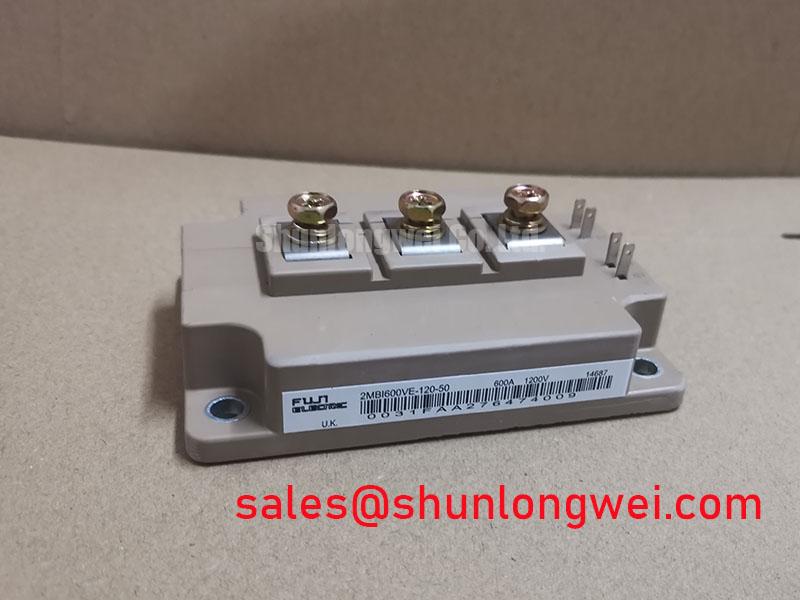
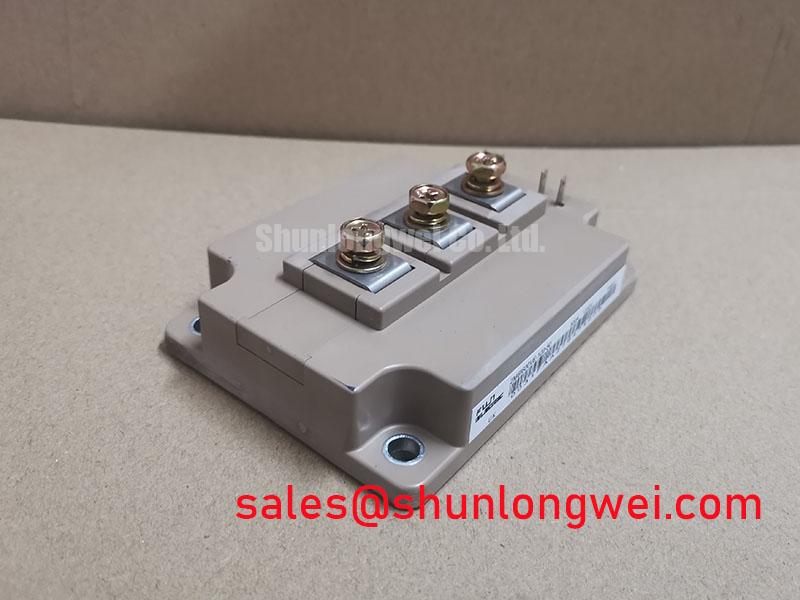
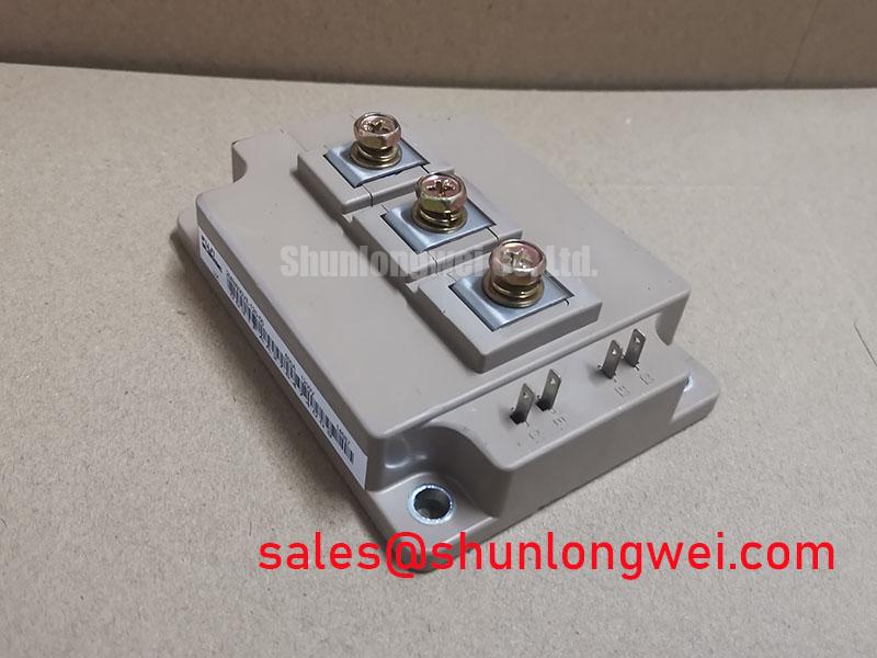
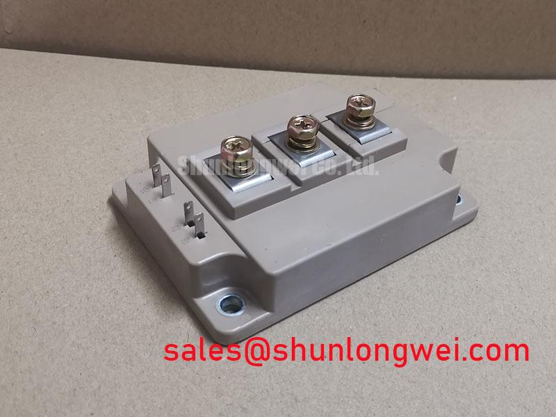
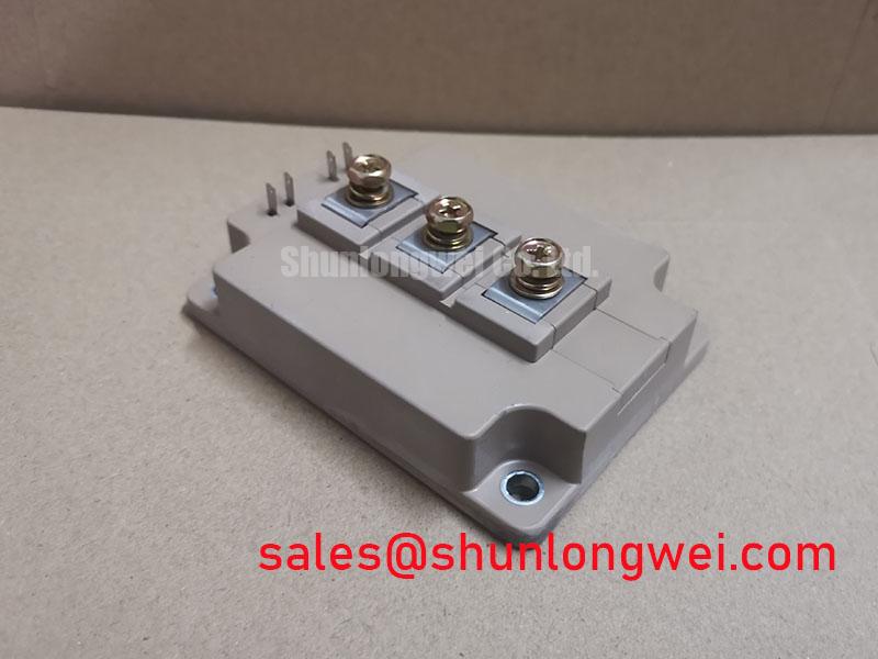
During a failed start or unexpected converter trip, isolate the DC link, discharge the energy storage network, and inspect the gate driver and power terminals before applying a replacement 2MBI600VE-120-50. The Fuji Electric unit is identified by an official rated voltage of 1200.0 V, an official rated current of 600.0 A, and a Fuji Power Module package. These are the available product identity parameters for initial replacement screening; actual operating limits remain dependent on the complete converter, cooling path, switching conditions, and protection coordination.
For a utility scale centralized battery energy storage PCS, the protection chain normally has to coordinate gate driver desaturation sensing, DC link protection, semiconductor fusing, and converter control logic. A desaturation detector can identify a rising collector emitter voltage during commanded conduction, but the detector threshold, blanking interval, filter behavior, and gate turn off response belong to the selected driver and system design. Treat a sub ten microsecond fault response as a Design Consideration for evaluating short circuit protection architecture, not as an official switching specification of this IGBT module.
Type I and Type II short circuit events can produce different current rise profiles and different stress on the IGBT, bus structure, and fuse. A practical commissioning procedure is to inject low energy test pulses first, verify that the driver recognizes abnormal VCE, and then examine the gate voltage and collector current together with a properly rated differential probe. A two stage soft turn off arrangement can reduce the rate at which current is interrupted and may limit inductive overvoltage. Its delay, gate resistance, clamp behavior, and energy capability must be selected from measured waveforms and the driver manufacturer’s data.
Semiconductor fuses should be coordinated with the converter’s prospective fault current and the module’s verified short circuit withstand data. The fuse I2t value is only meaningful when evaluated against the complete fault loop, including battery impedance, DC link capacitance, bus inductance, driver response, and clearing time. Do not treat a fuse rating as independent proof that the IGBT will survive a dead short. The system engineer should verify that the protection sequence prevents repeated fault pulses after the first trip.
Phase controlled rectifier sections upstream of a PCS can also affect the DC link ripple profile and the conduction angle seen by the power stage. When a rectifier operates with a delayed firing angle, the resulting current waveform can increase low order and high order grid harmonics unless the complete installation includes suitable filtering and control. The 2MBI600VE-120-50 should therefore be evaluated as one switching element within the converter topology, while harmonic compliance remains a property of the assembled equipment.
Transient Dynamics & Electrical Design: Negative Gate Bias Versus Active Miller Clamp on 2MBI600VE-120-50
High dv/dt at the collector can couple through the Miller capacitance and raise the gate potential of a device that should remain off. In a half bridge or bidirectional PCS leg, this can create unwanted cross conduction, abnormal current sharing, or repeated driver faults. The first diagnostic comparison should be made at the module gate and emitter reference pins, not only at the driver output connector, because common impedance in the return path can hide the actual gate waveform.
A dedicated active Miller clamp is an Engineering Recommendation for systems where measured common emitter movement or high dv/dt creates a credible false turn on risk. The clamp should engage only after the intended gate command has been removed and should be located close to the module’s gate return path. The driver supply, clamp transistor, gate resistor network, and protection return must be checked as one low impedance loop. A remote clamp connection can add parasitic inductance and reduce the benefit that the circuit is intended to provide.
Negative gate bias is another possible Design Consideration for suppressing unintended turn on. The commonly discussed negative bias range of −5 V to −15 V must not be treated as a confirmed rating for this specific module without the applicable Fuji Electric gate voltage specification. The integrator should verify the allowable gate emitter voltage, driver isolation, turn off clamp behavior, and transient overshoot before applying any negative rail. Excessive negative voltage can stress the gate structure even when the power circuit appears stable.
Desaturation protection should be checked for three separate events: the initial conduction blanking period, the recognition of abnormal VCE, and the controlled removal of gate charge. A response target below 3 microseconds may be used as a system evaluation point when selecting a protection architecture, but it is not an official parameter stated here for the 2MBI600VE-120-50. Two stage soft turn off can be considered when direct gate interruption produces excessive collector voltage overshoot. The correct sequence must be confirmed with current and voltage probes under the actual DC link and load conditions.
| Parameter | 2MBI600VE-120-50 | 2MBI600U4N-120-50 |
|---|---|---|
| Manufacturer | Fuji Electric | Fuji Electric |
| Official rated voltage supplied for listing | 1200.0 V | Consult the applicable product datasheet |
| Official rated current supplied for listing | 600.0 A | Consult the applicable product datasheet |
| Package description supplied for listing | Fuji Power Module | Consult the applicable product datasheet |
The comparison table is a screening aid rather than a substitution approval. Engineers assessing the related 2MBI600U4N-120-50 should compare terminal arrangement, electrical ratings, switching characteristics, thermal interface requirements, and the original driver configuration before selecting a replacement. A part number with a similar voltage and current label does not by itself establish mechanical or electrical interchangeability.
Fuji Electric’s public references on brake chopper IGBT modules and 7th Generation X Series IGBT modules provide useful background for comparing application families, but they should not be read as specifications for this exact part number.
2MBI600VE-120-50 Operational Boundaries: Evaluating High di/dt Gate Loop Induced Turn Off Limits
Separate the high current emitter connection from any auxiliary emitter or Kelvin style driver return shown in the original module drawing before routing the gate circuit. The main emitter path carries load current and develops a dynamic voltage drop from di/dt. A dedicated driver return, where provided by the verified terminal definition, allows the driver to sense the gate emitter voltage with less influence from the main power current path. The terminal identity must be taken from the correct Fuji Electric mechanical and electrical drawing for the purchased configuration.
In a PCS bridge, the gate loop should be kept physically close to the module terminals, with the outgoing gate path and its return arranged as a compact pair. The power commutation loop should remain distinct from the driver loop. This separation reduces the possibility that a high di/dt event will appear as a false gate command or disturb the desaturation reference. Layout clearance around the high voltage collector and DC link conductors must be established from the installation voltage, pollution environment, insulation system, and applicable equipment standard rather than from the module’s current rating alone.
When a converter reports intermittent shoot through, compare the gate emitter waveform at the module with the signal measured at the driver board. A difference between those locations may indicate common emitter inductance, connector movement, a damaged gate resistor, an unstable isolated supply, or probing error. Use a short measurement connection and verify both complementary channels during the same switching event. The diagnostic objective is to identify whether the false command originates in the control signal, the driver output stage, or the physical gate loop.
The auxiliary rectifier or precharge section can influence the gate driver supply during startup and fault recovery. A related device such as 1MBI300N-120 may appear elsewhere in the same system topology, but its presence does not define the drive requirements of the 2MBI600VE-120-50. The system integrator should verify isolation, supply sequencing, undervoltage lockout behavior, and fault reset logic for each power stage independently.
Bench Diagnostic: Disconnect control power before removing a gate cable or driver connector, then verify the discharged DC link with an appropriately rated meter before touching the module terminals.
Assembly Integrity & Layout Architecture: Implementing Heatsink Surface Flatness and Thermal Grease for 2MBI600VE-120-50
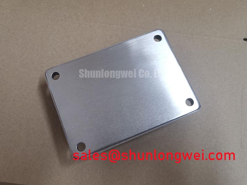
Thermal assembly begins with the mating surfaces, not with the module’s nominal current label. Inspect the heatsink for burrs, contamination, local dents, and visible bowing, then check the module baseplate and mounting region for damage. Surface flatness and cleanliness affect the thermal interface, while uneven clamping can place mechanical stress into the package and reduce contact over part of the base.
A thin, continuous thermal interface layer is a Design Consideration for reducing dry spots and trapped air. The often used 50 to 80 micrometre interface thickness should be treated as a general assembly starting point, not as an official Fuji Electric specification for this model. The selected compound, surface finish, pressure distribution, and application method determine the final result. Excess compound can increase thermal resistance and migrate toward nearby hardware.
Use the original mounting hardware and the manufacturer’s specified torque procedure when available. A calibrated diagonal cross pattern helps distribute pressure progressively across the baseplate. The general M5 mounting range of 2.5 to 3.5 N·m is an industry Design Consideration only and must not replace the applicable Fuji Electric installation instruction. Torque values vary with screw grade, washer design, thread condition, and mounting structure.
After assembly, inspect the baseplate seating and confirm that the heatsink remains mechanically stable during cable installation. Keep high voltage terminals, gate wiring, and auxiliary signal paths separated according to the system insulation design. The creepage and clearance required around the 1200 V class power circuit depend on working voltage, overvoltage category, pollution degree, altitude, material group, and the governing safety standard. The equipment designer must verify those distances in the finished PCS enclosure.
For long duration validation, record case temperature, heatsink temperature, gate waveform, fault events, and cooling system state under representative load cycles. The Field Engineer’s Handbook can support a structured approach to testing and failure analysis. It does not replace the Fuji Electric datasheet, the equipment safety file, or the measured limits established for the complete converter.