


Content last revised on September 10, 2026
6MBI75U4B-120-50 Thermal-Electrical Optimization: Optimizing Gate Drive Loop Geometry to Prepare Practical Tuning
Before reconnecting an inverter welder or medium frequency induction heating supply, isolate the DC link, inspect the module body and terminals, and verify the replacement marking against the equipment service record. A cold resistance comparison between the collector, emitter, and freewheel diode paths can identify an obvious abnormal reading, but it cannot by itself confirm dynamic switching health. Compare the suspected unit with a known good reference and use the original circuit diagram to identify each terminal before applying a gate signal.
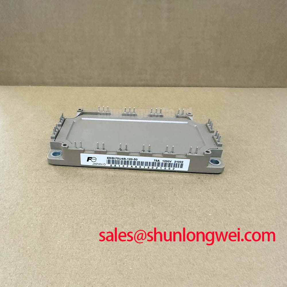
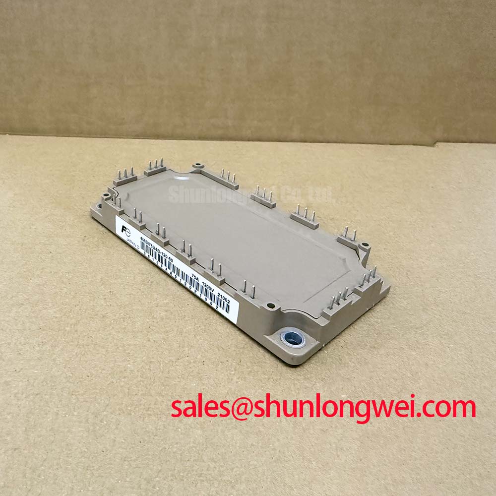
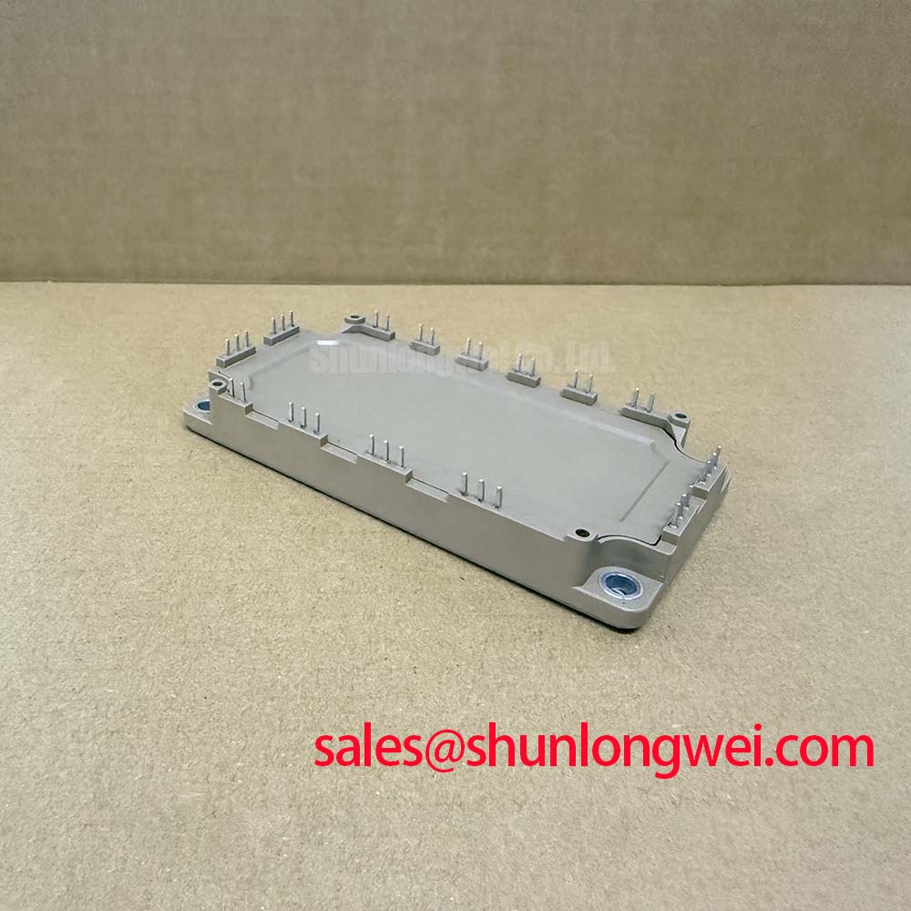
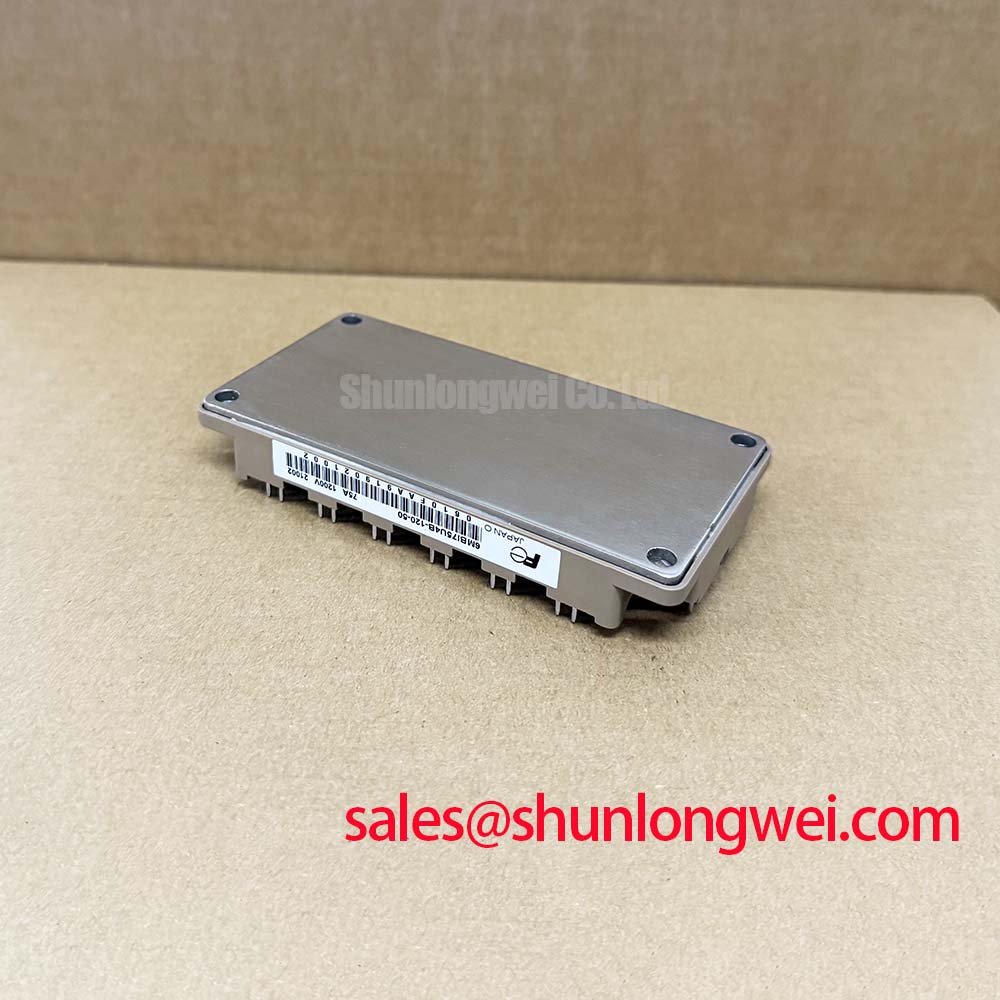
The Fuji Electric 6MBI75U4B-120-50 is a three phase IGBT module specified for a maximum collector emitter voltage of 1200 V. Its continuous collector current is 75 A at a case temperature of 80°C, while the listed collector emitter saturation voltage is 1.80 V typical and 2.20 V maximum at 75 A and 125°C junction temperature. These values are official specification data and should be checked against the switching frequency, current waveform, cooling arrangement, and DC link conditions of the equipment under repair.
When assessing conduction loss, do not use the nominal current rating as a substitute for an RMS thermal calculation. The load current may be pulsed, phase shifted, or limited by the control loop. An RMS current model is useful for estimating conduction heating, with the final result confirmed through case temperature measurement and the module thermal network. The general principles described in Root Mean Square current calculations can support this preliminary assessment, but the module’s actual junction temperature depends on switching loss, duty cycle, heat sink performance, and transient thermal impedance.
For the listed test condition of 75 A and 600 V, the official switching loss values are 10.0 mJ for turn on and 11.5 mJ for turn off. These figures are reference conditions rather than universal operating limits. A field engineer should capture collector emitter voltage and collector current together on an oscilloscope, then compare the measured switching waveform with the original design target. Ringing, excessive voltage overshoot, or an unusually extended current transition may result from gate loop impedance, busbar geometry, driver timing, or load commutation behavior.
Separate the auxiliary emitter return from the power path
Where the equipment wiring uses an auxiliary or Kelvin emitter connection, route that control return separately from the high current emitter path. The gate driver should reference the emitter point intended by the module’s terminal diagram, while the main current return should remain on the low impedance power circuit. Sharing a narrow control return with a rapidly changing load current can introduce mutual coupling and unwanted voltage movement at the driver reference. This can appear during testing as gate waveform distortion, uneven switching between phases, or intermittent driver protection.
Keep the gate loop compact, with the gate lead and its return routed together and away from the collector bus. Avoid routing the gate trace parallel to a high dv/dt switching node for a long distance. The exact clearance and conductor width remain system design decisions because insulation material, working voltage, pollution environment, and enclosure construction all affect the required layout. During troubleshooting, measure the gate to emitter voltage directly at the module terminals rather than at the driver board. This helps separate a driver output problem from voltage drop across the harness or emitter return.
The freewheel diode path also requires attention. The official forward voltage is 1.80 V typical and 2.20 V maximum at 75 A and 125°C. A diode conduction waveform that differs substantially from the expected commutation pattern should be investigated alongside the gate timing, current sharing, and DC link ripple. In a phase controlled front end, the rectifier conduction angle can change the DC link ripple and the harmonic current drawn from the mains. If an SCR stage is present, confirm its IGT, VGT, gate pulse width, and pulse train requirements from the SCR manufacturer’s documentation instead of transferring assumptions to this IGBT module.
⚠️ Field Alert: Disconnect the DC link and verify discharge before removing gate or power cables, because control terminals can be damaged by an energized or floating connection.
Preventing Spurious Faults: Dynamic Gate Impedance Control for Robust Guidelines for 6MBI75U4B-120-50
After the static inspection, check the gate driver with the power stage disabled. Confirm that each channel produces the intended gate to emitter waveform and that the complementary channels follow the controller’s interlock logic. A gate waveform that appears correct at the driver output may still be unsuitable at the module because common emitter inductance, cable coupling, and probe grounding can change the voltage seen by the IGBT die.
High dv/dt at the collector can capacitively inject current into the gate circuit. This may raise the off state gate voltage and create unwanted turn on in the complementary device. A dedicated active Miller clamp can reduce this risk when it is supported by the gate driver architecture. Its effectiveness depends on the driver’s clamp current, connection point, propagation delay, gate resistance, and power loop arrangement. Designers should verify the complete switching waveform under the highest expected current and voltage stress rather than treating the clamp as a standalone protection guarantee.
Negative gate bias is another possible design consideration for reducing susceptibility to parasitic turn on, but the usable value must come from the gate-emitter voltage rating, driver specification, isolation supply, and the module’s approved operating conditions. The supplied product data here does not establish a negative gate voltage rating for this specific module. The system integrator should therefore verify the gate voltage limits from the original Fuji Electric documentation before applying any negative bias.
Dead time should be long enough to accommodate driver propagation mismatch, turn off delay, gate discharge behavior, and the actual commutation path. Excessive dead time increases diode conduction and can increase recovery related stress; insufficient dead time can allow cross conduction. This is a control system parameter, not a fixed replacement value for the module. Tune it from measured collector current and voltage waveforms, with the thermal effect checked at the intended load profile.
Place the interlock signal path and isolated driver returns so that a switching node cannot inject a false transition into both channels. During a fault investigation, compare the high side and low side gate signals at the module pins, inspect the driver supply for collapse, and check whether the fault occurs at turn on, turn off, diode recovery, or a load transient. If the protection circuit trips only under power, use a properly rated differential probe and correlate the event with the current waveform rather than assigning a single cause from the fault code.
The module’s specified short circuit withstand time is at least 10 µs when Vcc is below 800 V and Vge is 15 V. This is official specification data for the stated condition, not permission to use repeated short circuit events as a production operating mode. The desaturation threshold, blanking interval, soft shutdown behavior, and fault reset sequence must be evaluated as a complete driver system. Repeated protection events should lead to controlled testing and root cause investigation, not automatic replacement of the module alone.
Transient Dynamics & Electrical Design: Galvanic Gate Drive Isolation, Reinforced on 6MBI75U4B-120-50
In a high voltage inverter welder or induction heating supply, the isolated gate driver must preserve the control waveform while its reference moves rapidly relative to the controller ground. Select the isolation barrier according to the equipment insulation coordination, working voltage, pollution degree, creepage, clearance, and applicable safety requirements. The supplied product information does not certify a particular driver barrier, reinforced isolation voltage, or common mode transient immunity. Those characteristics belong to the selected driver and complete assembly and must be verified from the driver manufacturer’s data and the equipment compliance plan.
Use a short, controlled connection between the isolated driver and the module gate terminals. Keep the isolated power supply loop separate from the collector switching loop, and avoid allowing the isolation transformer or DC to DC converter return to become part of the high current commutation path. A probe connected across the wrong reference can create a misleading gate waveform, so field measurements should be made with equipment rated for the common mode voltage and switching edge involved.
At the front end, a phase controlled rectifier can produce substantial low order and higher order current harmonics when its conduction angle is restricted by the DC link demand. The line reactor, DC link capacitor, firing control, and load profile jointly determine the input current spectrum. If an auxiliary rectifier or front end module is being reviewed, the 2MBI150UC-120 may be evaluated as a separate related power stage, subject to its own electrical specifications and the original topology. It should not be assumed to be a direct substitute for the 6MBI75U4B-120-50.
For service replacement, confirm the original gate polarity, phase sequence, driver supply arrangement, fault feedback, and mechanical terminal orientation. The manufacturer’s semiconductor information should be consulted alongside the equipment schematic; Fuji Electric’s power semiconductor reference information provides broader product context but does not replace the exact datasheet for this model.
When an isolated driver reports an undervoltage or desaturation event, inspect the isolation supply, gate return, driver timing, and current sensor path together. A fault that appears after warmup may also involve heat sink temperature, changing switching characteristics, or protection threshold drift. Record the event with synchronized voltage and current channels, then compare it with the known good phase. This approach provides usable evidence without treating one alarm indication as proof of one failed component.
6MBI75U4B-120-50 Circuit Protection & Reliability: Calibrating High Frequency Commutation Loop Inductance
During turn off, stray commutation inductance converts current change into a voltage overshoot. The engineering relationship can be described in the switching test as the DC link voltage plus the inductive contribution associated with loop inductance and current slew rate. The practical objective is to minimize the high current loop area, place the clamp or snubber where it can act on the actual switching path, and verify the peak collector emitter voltage at the module terminals.
Use a laminated or otherwise tightly coupled positive and negative DC bus arrangement where the equipment construction permits it. Keep the capacitor connection close to the module power terminals, maintain symmetrical phase geometry, and avoid long branch connections that add unequal inductance between parallel paths. The acceptable parasitic inductance is system determined. It must be established from the module voltage rating, operating DC link, current slew rate, snubber behavior, and measured overshoot rather than copied as a universal layout prescription.
Snubber selection also requires measurement. A capacitor that is too small may not control the transient, while excessive capacitance can increase switching current and loss. The resistor, capacitor, mounting inductance, pulse repetition rate, and thermal dissipation should be evaluated together. The official 1200 V VCES rating is an electrical boundary for the module; it does not eliminate the need to verify transient margin during the real switching sequence.
The listed per IGBT junction to case thermal resistance is 0.24 K/W. Use this official specification with the heat sink interface and cooling conditions to estimate steady state temperature, then account for switching and conduction losses. For pulsed welding or induction heating duty, a transient thermal impedance network is more appropriate than a steady state calculation alone. Measure the case temperature near the specified reference point and model the pulse width, repetition pattern, and recovery interval before judging junction temperature margin.
Inspect the heat spreading surface for flatness, contamination, and uneven pressure. Apply the interface material according to the equipment manufacturer’s assembly procedure, and tighten the mounting hardware in a cross pattern if the mechanical design requires it. Uneven pressure can increase thermal resistance and introduce mechanical stress, while excessive compound can reduce the effectiveness of the interface.
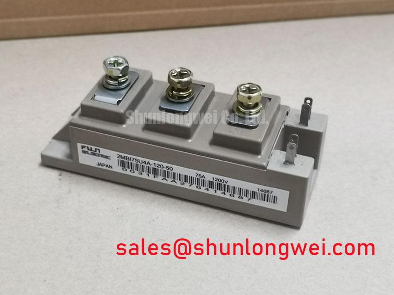
For cross model evaluation, engineers may compare the electrical role, current path, terminal arrangement, thermal interface, and gate drive requirements of the 2MBI300U4H-120-50. This is an engineering comparison point, not a substitute recommendation. The replacement decision should be based on the original circuit ratings, protection behavior, mechanical fit, and verified switching waveforms.
Long duration evaluation should use documented temperature cycling, load profiles, protection events, and electrical measurements. No field failure rate or service life should be inferred from the module’s nominal ratings alone. For broader discussion of industrial drive switching technology, engineers can consult Unlocking Efficiency in Industrial Drives, while treating any technology comparison as separate from the official specifications of this Fuji Electric part.
Before returning an inverter welder or medium frequency induction heating power supply to service, verify the collector emitter waveform, gate to emitter waveform, diode commutation, phase current balance, DC link ripple, heat sink temperature, and protection response under controlled load. The final acceptance limits are defined by the equipment design and applicable safety procedures.