

Content last revised on October 26, 2026
1MBI1600VC-120P Thermal-Electrical Optimization: Thermal Feedback Practical Tuning
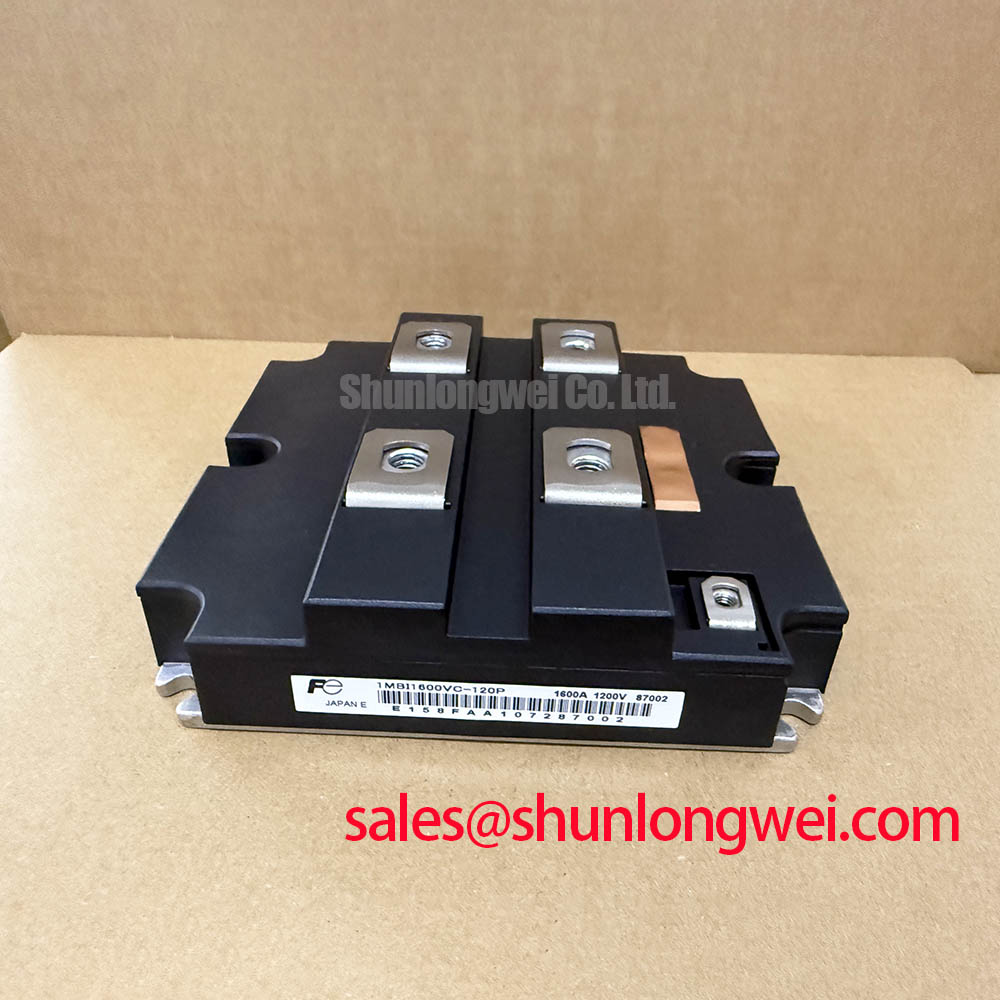
I would compare branch current and case temperature under the same stabilized load before changing gate resistance to address uneven sharing. For the Fuji Electric 1MBI1600VC-120P, the electrical and thermal limits below provide the starting point for that assessment. Record the case measurement position, cooling condition, and load alongside each reading so that subsequent maintenance measurements remain comparable.
| Official Specification | Value | Conditions |
|---|---|---|
| Collector-emitter voltage, VCES | 1200 V | Tj = 25°C |
| Continuous collector current, IC | 1600 A | Tc = 80°C |
| Collector-emitter saturation voltage, VCE(sat) | 2.10 V typical; 2.70 V maximum | IC = 1600 A, VGE = 15 V, Tj = 125°C |
| IGBT junction-to-case thermal resistance | 0.020 K/W maximum | Junction to case |
| Freewheeling diode junction-to-case thermal resistance | 0.036 K/W maximum | Junction to case |
| Short-circuit withstand time | At least 10 µs | Vcc = 600 V, VGE ≤ 15 V, Tj = 125°C |
| Maximum junction temperature | 150°C | Maximum junction-temperature limit |
Design Consideration: a positive VCE(sat) temperature coefficient can help steady-state sharing between parallel IGBTs when their operating point lies in the positive-coefficient region. A warmer branch then develops greater conduction voltage, tending to redistribute current. The single saturation-voltage test point above does not establish that region; temperature-dependent output curves are needed before relying on this mechanism. Unequal cooling or connection resistance can still dominate the measured distribution.
Dynamic sharing requires a separate check. Compare gate-loop geometry, driver propagation behavior, power-path impedance, and switching waveforms between branches. Symmetrical routing helps reduce differences, but equal cable length alone does not establish equal inductance. Maintain the equipment’s specified electrical clearances while keeping the gate and return paths closely coupled.
For procurement comparisons, the 1MBI300S-120 is a separate reference model, not an established replacement. Compare its ratings, circuit configuration, terminal drawing, and mounting interface independently. When evaluating the 1MBI1600VC-120P for a utility-scale centralized battery energy storage PCS, compatibility should be established against the installed converter’s electrical, mechanical, and cooling requirements.
Benchtop Waveform Tuning: Mitigating High-dv/dt-Induced Cross-Conduction Shoot-Through on 1MBI1600VC-120P
Capture the off-state gate-emitter waveform while the complementary switch changes state, using appropriately rated differential instrumentation and a short measurement loop. Design Consideration: collector-voltage transitions can couple current through gate-collector capacitance, raising the off-state gate voltage. Compare that excursion with switching current and driver behavior before attributing an observed disturbance to cross-conduction; probe pickup can resemble a genuine gate transient.
A low-impedance active Miller clamp can provide a local path for coupled gate current after turn-off. Its effectiveness depends on clamp engagement timing, connection inductance, and driver capability. Negative gate bias is another system-level option, but its magnitude must remain within the module’s gate limits and the driver’s operating envelope. Neither a clamp nor negative bias compensates for an unnecessarily long gate-return path.
Engineering Recommendation: assess dead time together with propagation tolerances, turn-off behavior, and diode commutation across the intended temperature range. Insufficient separation can permit overlapping conduction; excessive separation can increase diode conduction and alter converter behavior. The specified 10 µs minimum short-circuit withstand time applies only under its stated test conditions. It is not a permissible dead-time setting or a target delay for protection; sensing, decision, and turn-off behavior require coordinated validation.
During switching-frequency changes, compare semiconductor loss estimates with measured case temperature and cooling performance. Higher frequency increases the contribution of switching losses, so an unchanged load current does not imply unchanged thermal stress. Check filters, fan operation, recirculated exhaust, and inlet temperature before interpreting a hotter module as an electrical fault. The separate IGBT and diode thermal resistances should be applied to their respective loss paths.
For overvoltage control, evaluate local commutation-loop geometry and snubber behavior before assigning suppression to a MOV network. MOV coordination depends on clamping voltage at the relevant pulse current, absorbed energy, repetition, and connection impedance. It should not be assumed to suppress every fast collector-voltage peak. The Infineon EconoPACK™ Plus portfolio provides separate IGBT-module context, not Fuji-specific test evidence. Likewise, Infineon OptiMOS™ and CoolMOS™ power MOSFETs are different device families whose driver practices should not be transferred without device-level review.
Thermal-Interface Maintenance: Mitigating Thermal Grease Pump-Out on 1MBI1600VC-120P
Inspect the removed thermal-interface imprint and mating surfaces before applying fresh material. Uneven coverage, displaced compound, contamination, or localized dry regions can justify closer examination, but none identifies a unique failure mechanism by itself. Design Consideration: repeated thermal movement can redistribute interface material, while poor initial contact can produce similar temperature patterns.
Check heatsink flatness and the module’s specified mounting-surface geometry against the mechanical documentation. Do not assume a particular baseplate material, prescribed convexity, or universal flatness allowance. Remove residue without scratching the contact surfaces, and examine mounting threads and seating areas for damage that could prevent uniform loading. Mechanical correction should address the mating assembly rather than force the module against an unsuitable surface.
Engineering Recommendation: use an interface material and application method compatible with the specified assembly. Target continuous coverage without unnecessary thermal resistance, using the manufacturer’s requirements to determine quantity and finished thickness. Where the installation procedure specifies staged diagonal tightening, use a calibrated torque tool and follow that sequence. Mounting bolts and electrical terminals have different functions; their tightening requirements are not interchangeable.
Maintenance Note: Trend terminal temperature rise and inspect cooling airflow at planned service intervals, investigating changes before returning the equipment to sustained load.
After reassembly, compare case-to-heatsink temperature behavior under a repeatable operating condition. A change may reflect interface contact, airflow, load distribution, or sensor placement, so retain the operating context with the result. Set inspection intervals from equipment duty, contamination exposure, and observed trends rather than inventing a fixed grease-replacement period. In humid environments, address condensation through enclosure and operating procedures before energization.
Preventing Spurious Faults: Auxiliary Kelvin Emitter vs Main Power Emitter Guidelines for 1MBI1600VC-120P
Trace the driver return from the gate-driver board to the emitter connection identified in the manufacturer’s terminal drawing. Do not infer a Kelvin connection from terminal size or physical proximity. Design Consideration: where a dedicated auxiliary emitter connection is provided, keeping the driver return separate from the main load-current path reduces shared-inductance voltage in the gate loop.
A main emitter connection carries load current, while an auxiliary emitter return serves the gate-drive reference. Shared conductor inductance can shift that reference during rapid current changes, altering the effective gate-emitter voltage. Compare measurements at the module terminals with those at the driver output; a clean driver-board waveform does not establish that the same waveform reaches the device.
Keep gate wiring away from high-current commutation paths while preserving specified clearances and service access. Check return-path continuity, connector seating, and mechanical strain before changing protection thresholds to suppress intermittent trips. Correlate fault timing with switching events and measured gate behavior so that genuine protection operation is not mistaken for electrical noise.
The discussion of Resonant Topologies in Home Appliances offers background on topology-dependent switching conditions, not qualification evidence for this module or a PCS. For the installed assembly, retain the terminal map, driver-return routing, probe locations, and accepted waveforms in the maintenance record. Those references let the next inspection distinguish a changed connection from a changed operating condition.