

Content last revised on September 26, 2026
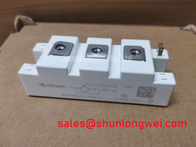
Transient Dynamics & Electrical Design: DC-Bus Low-Inductance Laminated Busbar Design on BSM100GAL120DLCK
For a commercial string inverter or micro-grid energy-storage converter, begin the electrical review at the commutation loop rather than at the nominal DC-link value. The turn-off voltage seen by the device is influenced by DC-bus voltage, stray inductance, and current slew rate. In engineering terms, the inductive overshoot rises with the product of loop inductance and current change rate, so the practical objective is to minimize the high-current loop and verify the resulting peak waveform during double-pulse or system switching tests.
A laminated busbar can help keep the outgoing and return current paths closely coupled. The capacitor connection, IGBT power terminals, and any braking chopper or inverter leg should be arranged to avoid unnecessary loop area. The required clearance and creepage distances remain system-dependent and must be selected for the working voltage, pollution environment, insulation system, and applicable safety standard. Do not treat a low-inductance layout as a substitute for voltage verification.
Where regenerative braking energy is transferred into a high-power braking resistor, the resistor, chopper leg, and local DC-link capacitor should be evaluated as one transient network. A snubber or active clamp may reduce overshoot, but its capacitance, damping, pulse energy, and thermal behavior require calculation from measured switching waveforms. Designers should confirm the peak collector-emitter voltage, ringing frequency, gate waveform, and resistor pulse duty under the worst credible operating condition.
During troubleshooting, compare a known-good phase leg with the suspect leg using an appropriate differential probe and carefully controlled grounding. Excessive ringing can also result from gate-loop coupling, probe placement, unequal busbar geometry, or a degraded capacitor connection. The FS100R12N2T4 may be evaluated as a separate, objectively comparable IGBT module option, but replacement suitability depends on terminal assignment, electrical ratings, thermal behavior, and mechanical compatibility.
Transient Dynamics & Electrical Design: Isolated DC-DC Power Supply Sizing for High-Immunity Gate Drive on BSM100GAL120DLCK
The isolated gate-drive supply should be assessed as part of the complete switching interface. Confirm the required gate voltage, negative-bias requirement if used, peak source and sink current, UVLO behavior, isolation rating, insulation coordination, and common-mode transient immunity from the driver manufacturer and the original equipment design. These are not established by the module’s 1200.0 V and 100.0 A ratings.
Keep the gate-drive loop physically compact and separate from the high-current collector and emitter path. If the package provides auxiliary or Kelvin-style terminals, the integrator should verify the exact terminal definition from the device drawing before routing the driver return separately. A separate sense return can improve measurement integrity, but only when its connection follows the confirmed module pinout and the driver reference is not unintentionally exposed to power-emitter voltage movement.
Miller plateau behavior and collector-emitter capacitance can transfer switching energy into the gate circuit. Gate resistance, ferrite damping, active Miller clamp operation, and the driver’s sink capability should therefore be tuned from measured gate and collector-emitter waveforms. A practical engineering recommendation is to verify turn-on and turn-off behavior at the intended DC-link voltage, load current, temperature, and switching frequency rather than selecting a gate network from nominal current alone.
Thermal derating also applies to the isolated supply, gate driver, module, busbar, and braking resistor. Switching losses generally vary with current, voltage, gate resistance, commutation path, and switching frequency. When evaluating a frequency range from low-kilohertz operation toward higher-frequency duty, designers should use measured or manufacturer-specified switching losses and confirm the cooling airflow, heatsink interface, and enclosure temperature. The BSM75GD120DLC can be considered as a neutral reference for a related rectification or front-end topology review, subject to its own documentation.
Benchtop Waveform Tuning: Mitigating Stress via Thermal Interface Material Thickness Uniformity on BSM100GAL120DLCK
Before waveform tuning, inspect the mounting surface, baseplate contact area, fastener condition, and thermal interface material application. Uneven contact can create localized thermal resistance and distort the relationship between electrical stress and measured temperature. The interface layer should be continuous and free from visible voids, while the selected material must be compatible with the module baseplate, heatsink finish, pressure distribution, and operating temperature.
Baseplate flatness and heatsink flatness should be checked according to the mechanical tolerances specified by the applicable module documentation. Do not compensate for a distorted mounting surface by excessive fastener force. Use the manufacturer’s recommended tightening sequence and torque where available; if that information is unavailable, the mechanical team should establish a controlled assembly procedure using the fastener size, thread condition, washer arrangement, and heatsink construction.
Safety Interlock Note: Disconnect the DC source and verify that the DC link has discharged before touching power terminals, gate-drive wiring, or measurement connections.
For benchtop tests, record gate-emitter voltage, collector-emitter voltage, current, heatsink temperature, and ambient conditions together. A waveform that changes after thermal soak may point to altered switching loss, driver supply movement, probe positioning, mounting pressure, or a thermal path issue rather than a single confirmed component fault. Recheck the signal path against a known-good assembly before changing gate resistance or clamp components.
When the module is used in a bidirectional DC-DC battery converter, repeated charge and discharge cycles can create thermal cycling in the semiconductor, interface material, soldered power connections, and busbar joints. The appropriate reliability review should combine measured temperature swing, dwell time, current profile, cooling response, and manufacturer reliability guidance. Avoid converting a short bench test into a claimed field-life prediction without qualified source data.
Transient Dynamics & Electrical Design: Atmospheric Neutron Radiation Impact on 1200 V IGBT Applications
Atmospheric neutron effects and single-event burnout are high-risk reliability topics that require qualified semiconductor reliability data, mission profile information, altitude exposure data, and device-specific analysis. The available product information establishes a 1200.0 V rated voltage and 100.0 A rated current for BSM100GAL120DLCK, but it does not establish a neutron-induced failure rate, FIT value, altitude derating curve, or guaranteed operating life.
For equipment installed at elevated sites, the design team should treat DC-link headroom as a verification topic rather than applying an assumed universal reduction factor. Measure the maximum bus voltage, switching overshoot, regeneration events, control fault response, and clamp behavior across the full operating envelope. The evaluation should include tolerance stack-up from the source, charging circuit, grid disturbance, battery operating range, and control reaction time.
In a micro-grid storage system, protection coordination should prevent a single abnormal switching event from exceeding the semiconductor voltage boundary. Designers should verify desaturation response, gate shutdown behavior, fuse or contactor coordination, braking-chopper operation, and the energy path during inverter faults. Any active clamp or surge-control network should be validated with high-bandwidth measurements and representative thermal conditions.
For a structured review of switching stress, thermal paths, protection concepts, and system reliability factors, consult the Power Electronics Masterclass. It should complement, not replace, the current Infineon datasheet, application documentation, certified insulation analysis, and test evidence for the actual converter.