Content last revised on October 14, 2026
FZ1600R12KL4C Field Inspection and Measurement Preparation
- With the DC link isolated and verified discharged, compare collector, emitter, and gate connections against the equipment schematic before taking cold-state measurements.
- Check terminal seating, mounting-surface condition, and cooling-interface contact before reconnecting the power busbars.
- Inspect the gate-drive return path and auxiliary supply connections for loose contacts or routing changes introduced during maintenance.
- Prepare suitably rated differential voltage and current probes before capturing switching or protection waveforms.
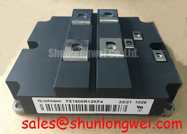
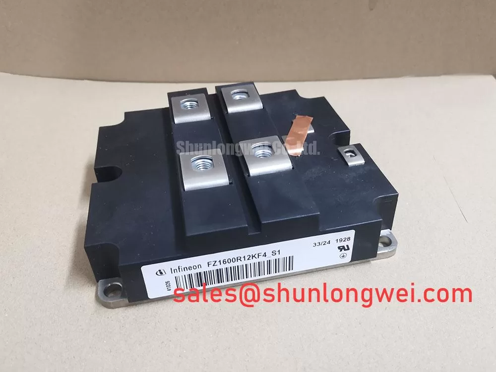
The FZ1600R12KL4C is an Infineon IGBT module with the following rated electrical boundaries. For a replacement assessment, record the complete device designation alongside the original driver, cooling assembly, and power-terminal arrangement.
| Parameter | Value | Classification |
|---|---|---|
| Model | FZ1600R12KL4C | Product designation |
| Manufacturer | Infineon | Manufacturer identity |
| Rated voltage | 1200 V | Official Specification |
| Rated current | 1600 A | Official Specification |
| Package | Module | Official Specification |
| Dynamic, thermal, and mechanical limits | Consult Datasheet | Conditions required for integration assessment |
Field Diagnostics & Commissioning: Diode Softness Factor Optimization in FZ1600R12KL4C Topologies
Capture the commutating diode current together with collector-emitter voltage to distinguish reverse-recovery behavior from measurement-loop ringing. As a Design Consideration, reverse-recovery peak current, commonly designated I_rrm, and the recovery-tail slope should be assessed at representative current and temperature conditions. A sharply collapsing recovery current can excite stray inductance, but an oscillatory trace alone does not establish diode damage.
Softness-factor comparisons require consistent definitions of the recovery intervals and consistent test conditions. Treat “Sy” as a circuit or test-document label unless its definition is established; it is not an additional verified FZ1600R12KL4C specification. Probe placement matters here: a long measurement loop can exaggerate the apparent voltage spike and obscure the recovery tail.
As an Engineering Recommendation, evaluate turn-on gate resistance and any RC snubber together. Slower commutation can reduce recovery stress while increasing switching loss; additional snubbing introduces dissipation and changes the transient current path. Select adjustments through controlled waveform comparisons rather than assigning a universal resistor or capacitor value. Preserve the equipment’s required electrical clearances when positioning snubber connections near the switching loop.
For circuit-context comparison, the FF200R12MT4 can be reviewed as another module in a separate converter leg or associated subsystem, subject to the actual schematic. It should not be assumed to be a passive front-end rectifier or a direct substitute. The Infineon IGBT Modules & Discretes Official Portfolio provides manufacturer context for distinguishing module configurations.
Preventing Spurious Faults: DC-Link Capacitance Bank Layout and Low-ES Guidelines for FZ1600R12KL4C
Trace the high-current commutation path from the local DC-link capacitor through the switching devices and back to the capacitor. As a Design Consideration, capacitor-bank performance depends on connection inductance as well as capacitance and equivalent series resistance. A remotely mounted bank can support bus energy storage while leaving the local switching loop exposed to appreciable transient voltage.
The relevant Engineering Calculation is that peak switching voltage approximately equals DC-link voltage plus loop inductance multiplied by current slew rate. This simplified relationship explains why compact opposing current paths and balanced planar busbar connections help control overshoot; it does not establish a universal allowable loop inductance. Determine the voltage margin from measured peaks, operating conditions, and the device’s applicable limits.
Practical tip: Favor balanced, closely coupled outgoing and return busbar paths, then verify turn-off voltage margin with a representative double-pulse test.
Gate-driver sourcing and sinking capability should be evaluated against the charging and discharging demands of the selected module. As an Engineering Recommendation, inspect gate-voltage ringing alongside collector current before changing external gate resistance. Excess damping can slow switching unnecessarily, while insufficient damping can leave the gate loop sensitive to coupled transients. Snubber selection should likewise include pulse loading, repetitive dissipation, and physical connection length.
During cross-model assessment, compare FZ1800R12KL4C with FZ1600R12KL4C for terminal geometry, driver loading, switching characteristics, and cooling requirements rather than treating the designation as proof of interchangeability. Potential assessment contexts include high-speed rail and heavy-freight locomotive traction inverters, subject to equipment-specific qualification.
Preventing Spurious Faults: Gate-Driver Auxiliary Power Sequencing Guidelines for FZ1600R12KL4C
Observe auxiliary supply startup, driver undervoltage lockout, and gate-emitter voltage before enabling the DC link. As an Design Consideration, the driver should establish its intended disabled state before the power stage encounters bus voltage. Check shutdown sequencing as well: removing auxiliary power must not leave the gate uncontrolled while stored DC-link energy remains.
Miller coupling can inject gate current during rapid collector-voltage transitions. Reverse-transfer capacitance, often designated C_res, is a voltage-dependent capacitance rather than a gate-charge quantity. Its influence should be considered alongside the driver’s sink path, gate-return inductance, and the actual gate waveform. An active Miller clamp or negative off-state bias requires coordinated driver design; neither a particular bias voltage nor clamp threshold follows from the module’s headline ratings.
As an Engineering Recommendation, examine the interval between auxiliary supply collapse and the removal of switching permission. Intermittent resets can arise from supply disturbance, interlock behavior, or coupled noise, so correlate driver status signals with local supply and gate measurements. Route the gate return away from power-current paths, preserving insulation spacing determined by the assembly’s voltage and environmental requirements.
The Infineon PrimePACK™ portfolio offers context for other module platforms, not evidence that FZ1600R12KL4C belongs to that package family. Driver-interface and mechanical compatibility remain separate assessment tasks.
FZ1600R12KL4C Operational Boundaries: Evaluating Desaturation Detection Limits
Measure protection timing from fault onset through detection, driver response, and current extinction rather than recording only the desaturation comparator transition. As a Design Consideration, a fault present at turn-on and a fault developing during conduction can produce different detection conditions. Blanking, sensing-network response, and driver propagation delay all contribute to the total protection interval.
Desaturation sensing must distinguish elevated collector-emitter voltage during a fault from legitimate switching transients. Increasing blanking can suppress nuisance trips but also delays protection. Assess that tradeoff against the module’s specified short-circuit operating conditions, without assigning a generic short-circuit withstand time to FZ1600R12KL4C.
As an Engineering Recommendation, evaluate controlled or staged fault turn-off where the driver supports it. Reducing abrupt current interruption can limit inductive overshoot, but slower shutdown also extends fault-energy deposition. Use a controlled validation arrangement with appropriate containment and instrumentation; deliberate short-circuit testing is not a routine field diagnostic.
Repeated protection events also warrant inspection of cooling contact and temperature recovery before another energization attempt. Diode surge capability and junction-temperature recovery are separate limits from rated module current. For broader cooling-interface principles, The Advanced Thermal Management Revolution provides background without establishing this module’s internal construction. Record the fault waveform, cooling condition, and driver response together so the next repair decision addresses observed evidence.