
Content last revised on October 11, 2026
FZ1600R12KF4 Identification and Pre-Installation Checks
- Isolate the power stage, verify that the DC link is discharged, and inspect the module terminals before connecting resistance or diode-test instruments.
- Check the module mounting face and heatsink for contamination, surface damage, and uneven contact before disturbing the fastening arrangement.
- Trace the gate-drive connections against the equipment schematic, including the emitter return, auxiliary supply, and protection feedback path.
- Match the complete FZ1600R12KF4 part designation and electrical ratings to the equipment repair specification before evaluating a replacement.
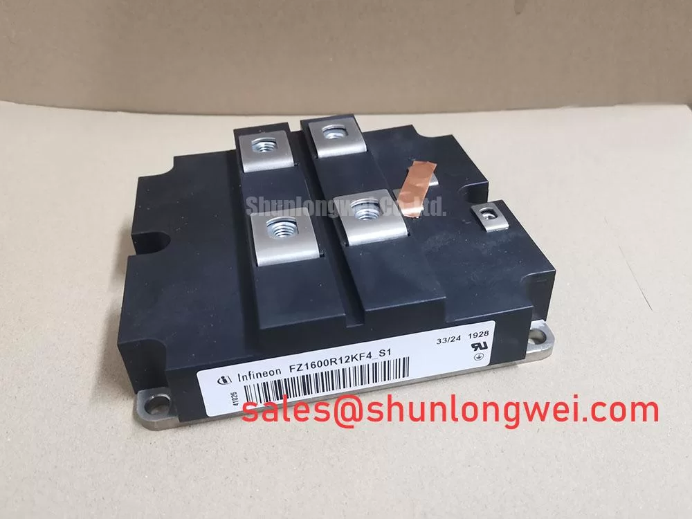
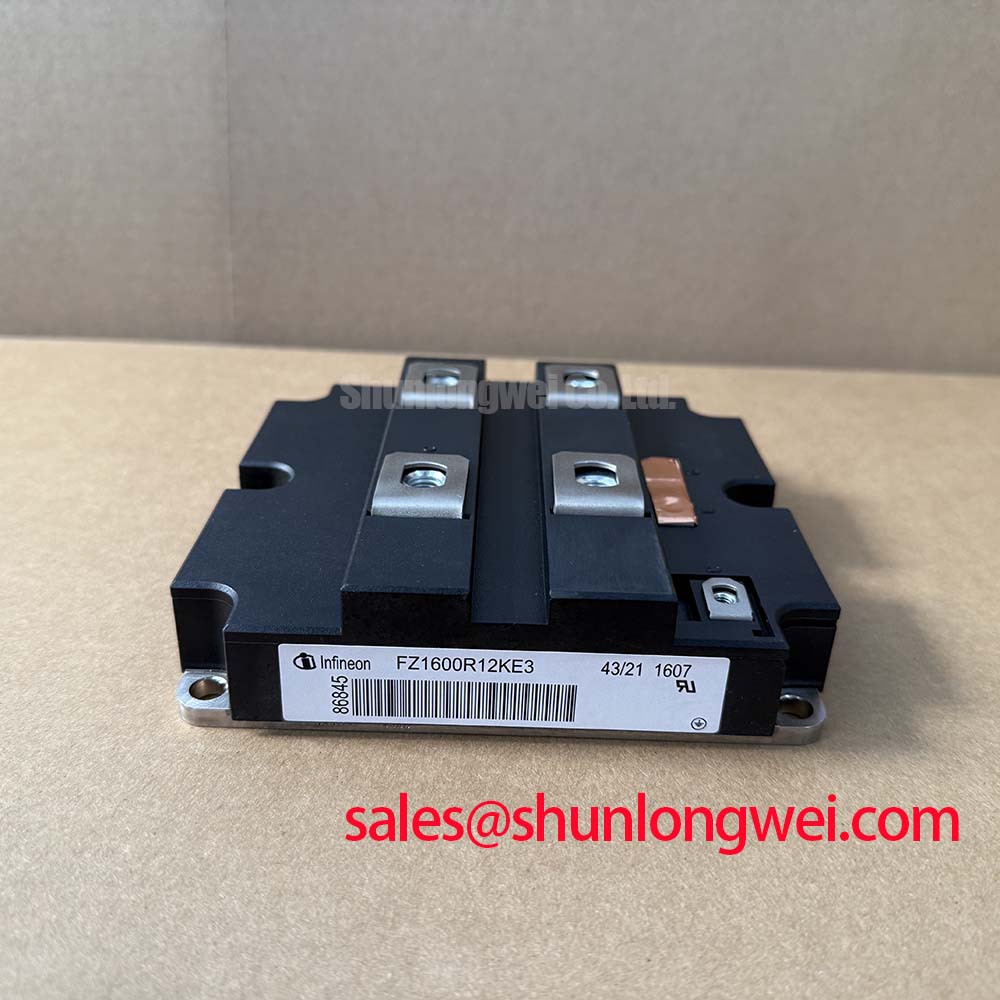
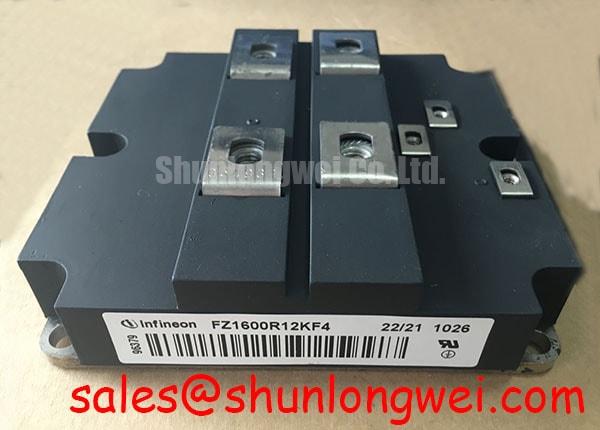
The Infineon FZ1600R12KF4 is an IGBT module with a specified collector-emitter voltage rating of 1200 V and a rated collector current of 1600 A under the datasheet-specified conditions. These ratings establish its basic electrical identity; integration also depends on the mounting interface, gate-driver behavior, thermal conditions, and fault protection of the equipment receiving it.
| Product attribute | Value | Parameter identity |
|---|---|---|
| Model | FZ1600R12KF4 | Product designation |
| Manufacturer | Infineon | Manufacturer identification |
| Collector-emitter voltage rating | 1200 V | Official Specification |
| Rated collector current | 1600 A, under datasheet-specified conditions | Official Specification |
| Package | Module | Official Specification |
| Mechanical dimensions, terminal assignments, thermal limits, and switching test conditions | Consult Datasheet | Required integration references |
For procurement records, the FZ1600R12KF4 product page provides a model-specific reference. Keep the equipment position, removed-part designation, and associated driver assembly together in the repair record so that purchasing and commissioning teams evaluate the same configuration.
FZ1600R12KF4 Circuit Protection & Reliability: Preventing Mounting-Induced Substrate Damage
Check mounting-face flatness and the heatsink contact surface before tightening the FZ1600R12KF4 into position. As a Design Consideration, uneven support can concentrate mechanical loading and create inconsistent thermal contact. Evaluate apparent convexity against the specified mounting geometry rather than treating every departure from flatness as a defect; deliberate geometry and damage require different decisions.
Remove old thermal-interface residue without scoring the mating surfaces. Inspect around fixing points for raised edges, trapped debris, and evidence that previous hardware loaded the housing unevenly. A module that rocks on the heatsink before fastening deserves further examination of both surfaces. Increasing bolt force is not a sound method of correcting an unsuitable mating surface.
Thermal-interface material should fill surface irregularities without becoming an uncontrolled spacer. Select its application method and coverage from the approved module and interface-material instructions. A generic film-thickness target is not an official FZ1600R12KF4 requirement. Excess material can obscure poor contact, while incomplete coverage can leave localized thermal resistance that is difficult to recognize from coolant temperature alone.
As an Engineering Recommendation, use a calibrated fastening tool and the documented tightening sequence, distributing engagement progressively across the mounting points. A diagonal sequence can help distribute loading where the mounting instructions permit it, but the specified hardware, washers, and final torque remain decisive. Do not transfer press-pack clamping methods, spring-stack pressures, or double-sided cooling assumptions to this module without an applicable mechanical specification.
Keep busbar alignment separate from heatsink fastening. Main terminals should not be used to pull a displaced conductor into position, because the resulting mechanical load can remain after the mounting bolts are correctly tightened. Check conductor support and access clearance before final assembly. Terminal clearance must follow the equipment insulation design, including pollution conditions and conductor geometry, rather than a universal spacing rule.
After reassembly, compare temperature behavior under controlled loading with the equipment baseline. An unexpectedly warm region may justify checking interface coverage, cooling distribution, or electrical loading; it does not identify a single failure mechanism. Record mounting materials and fastening settings so that later thermal observations can be related to a reproducible assembly process.
FZ1600R12KF4 Thermal-Electrical Optimization: Protection Coordination and Practical Tuning
Compare the semiconductor fuse’s total clearing behavior with the complete DC-link fault path before accepting the protection arrangement. As a Design Consideration, fuse selection involves prospective fault current, DC voltage, interruption capability, and the energy delivered before clearing. A fuse current rating alone does not establish protection of the FZ1600R12KF4.
The fuse’s total clearing I²t is relevant to energy coordination, but it is not automatically equivalent to an IGBT short-circuit withstand specification. Gate-controlled short-circuit behavior depends on operating conditions and protective turn-off, while fuse interruption follows its own time-current and arc-clearing characteristics. Compare compatible manufacturer data and system fault calculations rather than deriving module survivability from the 1600 A rating.
Separate rapid electronic protection from upstream interruption. Driver fault detection should initiate the equipment’s validated shutdown response; the fuse addresses faults within its specified interruption envelope. Capacitor discharge paths, busbar impedance, and fault location influence which element acts first. Neither element should be described as guaranteeing that the module enclosure remains intact under every short circuit.
The phrase “Type-2 coordination” should not be treated as an inherent certification of this IGBT module. Any coordination claim belongs to a defined assembly, protection combination, and applicable test basis. For repair acceptance, retain the equipment protection specification and verify that the installed fuse and driver configuration still match it.
Complementary gate interlocking addresses a different hazard: simultaneous conduction caused by command overlap or unequal switching delays. As an Engineering Recommendation, determine dead time from the relevant turn-off behavior, driver propagation variation, and controller timing under operating temperature and supply conditions. An arbitrary timing buffer can either leave insufficient separation or introduce excessive waveform distortion.
Observe both complementary gate signals during command transitions and protection events. Check whether a fault forces both commands into the intended inhibited state and whether restart requires the prescribed reset sequence. Noise on a shared return or poorly routed interlock signal can complicate this behavior, so review the actual wiring rather than only the controller settings.
If the equipment includes a MOV-based overvoltage network, evaluate its clamping behavior, energy duty, and location within that existing protection architecture. A remote MOV cannot be assumed to control the fast overshoot at the module terminals. Local switching stress and wider DC-link surge protection should be assessed separately, with each protective element checked against its own operating conditions.
Assembly Integrity & Layout Architecture: Implementing DC-Bus Operating Voltage Headroom Derating for FZ1600R12KF4
Measure collector-emitter voltage at the module during switching transitions when assessing DC-bus operating headroom. The 1200 V rating is the electrical boundary relevant to the device; the operating assessment must include bus variation, transient overshoot, and the conditions associated with the manufacturer’s limits. Use a suitably rated differential measurement arrangement with controlled probe-loop geometry.
As a Design Consideration, reduce commutation-loop inductance to limit the voltage generated by rapid current change. Closely coupled outgoing and return conductors can help, but the benefit depends on the complete capacitor-to-module path. Examine joints, conductor transitions, and connections shared between switching positions, not just the apparent symmetry of the main busbar.
Practical design tip: Favor a short, balanced commutation path, then validate turn-off voltage headroom through double-pulse measurements using the intended busbar and driver assembly.
Keep altitude-related reliability assessment distinct from ordinary switching overshoot. As a Design Consideration, elevated installation sites can warrant review of atmospheric-radiation effects alongside cooling and insulation requirements. Numerical single-event burnout or FIT predictions require device-specific susceptibility data and an applicable environmental model; no such rate should be inferred from the voltage rating or part designation.
The Infineon IGBT Modules & Discretes official portfolio provides manufacturer context for the device family. For supporting device-physics explanations during reliability reviews, The Ultimate IGBT Knowledge Base can supplement the module documentation without replacing product-specific qualification evidence or establishing a service-life guarantee.
When assessing integration into a utility-scale centralized battery energy storage PCS, designers should compare bidirectional current paths, switching conditions, cooling capability, and fault response with the original power-stage specification. This is a compatibility evaluation, not a claim that the module is qualified for every PCS architecture.
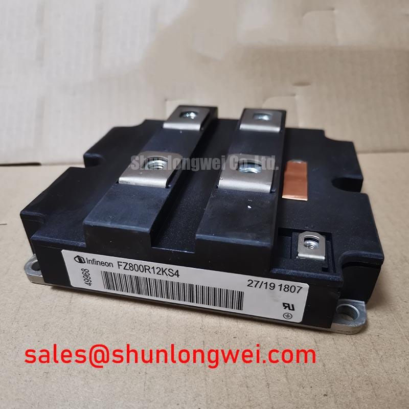
For repair sourcing, the related FZ800R12KS4 belongs in a separate engineering comparison, not an automatic substitution instruction. Compare current capability, circuit configuration, terminal geometry, mounting interface, thermal performance, and gate-drive requirements before considering any change. A related model name does not establish interchangeability, and an equipment-approved bill of materials remains the practical starting point.
Benchtop Waveform Tuning: Mitigating Stress via Floating Gate Bias Supply Decoupling on FZ1600R12KF4
Verify that the floating gate-driver supply reaches its valid operating state before the control system permits DC-link energization. As an Engineering Recommendation, inspect the interaction between auxiliary power, undervoltage lockout, controller enable, and contactor sequencing. The inhibited state should remain defined during startup, shutdown, and interrupted auxiliary power.
Negative turn-off bias, where used by the validated driver design, must remain within the module’s gate-voltage limits throughout transitions. It is not a universal prescription for this model. Evaluate the actual off-state voltage at the gate relative to its associated emitter return, including supply ripple, switching disturbances, and the interval during which the floating supply loses regulation.
Place driver decoupling within the local current path specified by the driver design. Long supply connections can introduce impedance between the source and the output stage, producing rail disturbance during gate charging and discharging. Check both the supply waveform and gate waveform under the same operating event so that an apparent gate anomaly is not mistaken for a command-timing problem.
Miller-induced gate movement should be assessed during complementary-device switching, particularly when collector voltage changes rapidly. As a Design Consideration, gate-loop routing, return-path impedance, driver sink behavior, and any implemented clamp arrangement influence susceptibility to unintended turn-on. Observe the gate at the module connection rather than relying solely on measurements taken at the driver board.
Include auxiliary-supply interruption and controlled restart in the bench test. Record gate behavior, driver fault status, and controller enable together, checking that no unintended pulse appears while the bias supply passes through its undervoltage region. Increase test stress only through the equipment’s validated commissioning procedure, retaining the waveform records that establish acceptable switching and interlock behavior.