

Content last revised on October 12, 2026
Assembly Integrity & Layout Architecture: Implementing Derating Guidelines for FZ800R12KS4
- Isolate the traction inverter and confirm cold-state terminal impedance before applying any gate signal.
- Inspect the mounting interface, thermal compound coverage, clamp flatness, and parallel power-path symmetry.
- Check gate-driver isolation, return-path continuity, interlock operation, and connector seating.
- Capture collector-emitter voltage and gate-emitter voltage during controlled switching before full-load commissioning.
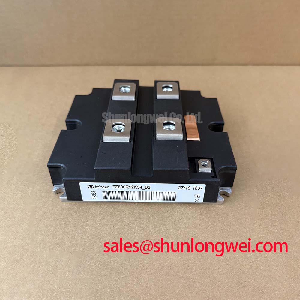
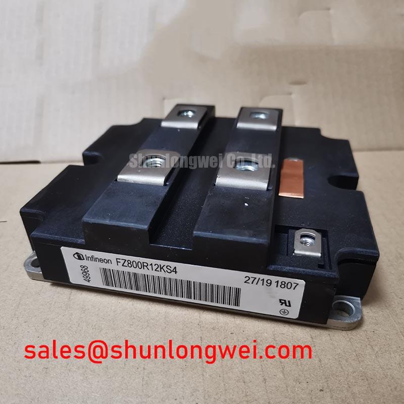
FZ800R12KS4 is an Infineon 1200 V, 800 A IGBT module intended for high-power converter evaluation where switching stress, thermal transfer, and current sharing must be verified at system level. Its official electrical ratings include VCES = 1200 V at Tvj = 25°C, IC nom = 800 A at TC = 80°C, and ICRM = 1600 A for a 1 ms repetitive peak current condition.
| Official parameter | Value | Specified condition |
|---|---|---|
| Collector-emitter voltage | 1200 V | Tvj = 25°C |
| Continuous DC collector current | 800 A | TC = 80°C |
| Repetitive peak collector current | 1600 A | tp = 1 ms |
| Total power dissipation | 7600 W | TC = 25°C, per IGBT |
| Repetitive peak reverse voltage | 1200 V | Tvj = 25°C |
| Collector-emitter saturation voltage | 3.20 V typical, 3.70 V maximum | IC = 800 A, VGE = 15 V, Tvj = 125°C |
| Gate-emitter leakage current | 400 nA | VCE = 0 V, VGE = 20 V, Tvj = 25°C |
| Turn-on energy loss per pulse | 76.0 mJ | IC = 800 A, VCE = 600 V, Tvj = 125°C |
| Turn-off energy loss per pulse | 58.0 mJ | IC = 800 A, VCE = 600 V, Tvj = 125°C |
| Junction-to-case thermal resistance | 16.5 K/kW | 0.0165 K/W per IGBT |
| Case-to-heatsink thermal resistance | 13.5 K/kW | 0.0135 K/W per IGBT with paste |
The first layout decision is to keep the commutation path short, symmetrical, and mechanically stable while applying system-level derating to voltage, current, switching frequency, and temperature. The stated VCES rating of 1200 V is an official device limit, not a target operating point for an uncontrolled DC link. Engineers should measure the maximum collector-emitter excursion at the module terminals during the fastest relevant switching event and compare it with the complete converter protection strategy.
The positive temperature behavior of VCE(sat) at high current can support static current sharing between paralleled IGBTs when the devices, gate circuits, busbar geometry, and thermal paths are closely matched. This benefit does not automatically correct dynamic imbalance. Unequal gate-loop inductance, different emitter return paths, or asymmetric busbar inductance can cause one device to turn on or off earlier than another. Route each gate and return conductor with comparable geometry, avoid shared high-current emitter sections, and inspect the mechanical position of each module relative to the laminated busbar.
For traction inverter repair or retrofit evaluation, the mechanical interface deserves the same attention as the semiconductor rating. Confirm heatsink flatness, contact coverage, fastener sequence, and paste distribution before interpreting thermal data. The published RthCH = 13.5 K/kW applies with paste under the stated specification condition; contamination, voids, surface tilt, or excessive compound thickness can increase the actual case-to-heatsink thermal path.
💡 Pro Tip: Keep the positive and negative power paths physically balanced and confirm turn-off overshoot with a properly rated differential probe before increasing load.
When comparing system architecture, the FZ1600R12KL4C can be reviewed as a separate high-current module option, but voltage, current, thermal, gate-drive, and mechanical compatibility must be evaluated from the original converter design rather than inferred from the part number.
Benchtop Waveform Tuning: Mitigating High-dv/dt Cross-Conduction and Shoot-Through on FZ800R12KS4
High dv/dt can transfer displacement current through the inactive switch gate loop and create an unintended rise in gate-emitter voltage. In a half-bridge, that event can overlap with the commanded turn-on of the complementary device and produce cross-conduction. The appropriate response is to examine the complete gate-loop waveform, including the driver output, gate-emitter voltage at the module pins, and the timing relationship between the two complementary channels.
A dedicated low-impedance active Miller clamp is a design consideration where the converter experiences strong common-source or collector-emitter transients. A negative off-state gate bias may also be evaluated when the gate-driver manufacturer, insulation system, and module gate-emitter limits support it. The negative bias value must be selected by the system designer from the verified driver capability and the module’s permitted gate-emitter range; it should not be treated as an automatic prescription for every installation.
Dead-time should be established from measured turn-off behavior, driver propagation mismatch, temperature, load current, and the recovery behavior of the complementary commutation path. Excessive dead-time can increase diode conduction and switching loss, while insufficient dead-time can allow simultaneous conduction. Use an interlock structure that prevents contradictory commands even during controller reset, auxiliary supply interruption, or signal corruption.
The gate driver and power stage should be commissioned at reduced energy first. Observe whether gate voltage remains stable during the opposite switch transition, then check the collector-emitter waveform for abnormal ringing and current overlap. In a system that also includes a controlled rectifier or front-end power stage, the switching supply arrangement can be reviewed alongside the FF400R12KL4C as a separate complementary topology reference, without assuming interchangeability.
Active clamp behavior, gate resistor selection, and pulse shaping should be tuned against measured switching energy. The official reference conditions for this module list Eon = 76.0 mJ and Eoff = 58.0 mJ at IC = 800 A, VCE = 600 V, and Tvj = 125°C. Actual converter losses will vary with gate resistance, stray inductance, current commutation, temperature, driver voltage, and circuit layout.
FZ800R12KS4 Thermal-Electrical Optimization: Overvoltage Trip Prevention via Fast-Switching Practical Tuning
DC-link overvoltage during motor deceleration is a system energy-management problem. The braking IGBT and ballast resistor must be selected from the motor inertia, speed profile, regenerative energy, duty cycle, DC-link capacitance, braking response, and permitted voltage window. The module’s ICRM = 1600 A rating for a 1 ms repetitive peak condition cannot be converted directly into a resistor or braking-duty specification.
During commissioning, record DC-link voltage at the capacitor bank and at the switching module because wiring inductance can create a local transient that is not visible at the controller measurement point. Confirm that the braking command arrives before the protective threshold, that the resistor remains within its thermal duty capability, and that the braking path does not share an unnecessarily inductive loop with the traction commutation path.
Fast switching can reduce transition loss but may increase voltage overshoot and electromagnetic coupling. A laminated busbar, controlled commutation loop, and physically separated control wiring are useful design considerations. The final balance between switching speed and transient stress should be established through controlled pulse testing across the intended temperature and load range.
Traction applications may also include phase-controlled rectifiers, whose firing angle influences DC-link ripple, input power factor, and harmonic current. Gate triggering for a thyristor front end must be based on its verified IGT, VGT, pulse width, and pulse-train requirements. Those trigger characteristics belong to the selected thyristor and gate unit, not to the FZ800R12KS4 IGBT module. Grid harmonic mitigation therefore requires system-level filter, control, and compliance assessment rather than a claim assigned to this module alone.
Field Diagnostics & Commissioning: Transient Thermal Impedance in FZ800R12KS4 Topologies
Peak junction temperature under pulsed overload should be derived from the actual switching and conduction loss profile, not from the continuous current rating alone. The official RthJC = 16.5 K/kW value is given per IGBT, while the published Ptot = 7600 W applies at TC = 25°C per IGBT. A transient thermal model must therefore include pulse duration, repetition pattern, case temperature, heatsink response, and the thermal interaction between devices.
For practical commissioning, calculate conduction loss from the measured current waveform and the temperature-relevant VCE(sat) condition, then add switching losses based on the actual voltage, current, gate timing, and junction temperature. A multi-RC network can represent transient junction-to-case behavior when the manufacturer’s thermal impedance curves or validated model are available. The predicted junction temperature should be checked against the measured case temperature and the converter’s protection response.
If the case temperature rises while electrical waveforms remain apparently normal, inspect thermal interface pressure, paste spread, mounting flatness, airflow, and sensor placement. If collector-emitter overshoot increases with temperature or load, return to the commutation loop and gate timing rather than assigning the symptom to thermal resistance alone. A field measurement plan should capture current, VCE, VGE, case temperature, DC-link voltage, and fault timing on the same time base.
High altitude, cosmic-ray-induced single-event effects, short-circuit endurance, FIT data, insulation reliability, and lifetime prediction require application-specific evidence and should not be assigned numerical margins without an authoritative source. For gate-drive development and long-duration test planning, the Evolution of Negative Off-Bias Gate Drive Circuits provides relevant background for evaluating off-state control strategies. The Infineon IGBT Modules Overview and the Infineon RCDC application note can also help separate device-specific behavior from broader converter topology considerations.
For potential evaluation in high-speed rail or heavy freight locomotive traction inverters, the replacement decision should include electrical rating, gate-driver compatibility, thermal interface, busbar geometry, protection timing, and documented switching-test results. Procurement teams should match the module marking, package interface, and approved system documentation before release to service.