Content last revised on October 12, 2026
Field Diagnostics & Commissioning: Screening Substrate Ceramic DBC Micro-Crack in FZ1800R12KL4C Topologies
- Record the cold state condition of the main terminals before applying any test voltage.
- Confirm that the module mounting surface, thermal interface, and baseplate contact are clean and mechanically even.
- Check gate circuit isolation and connector polarity against the original converter wiring documentation.
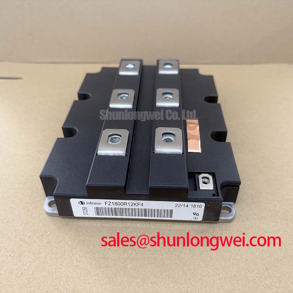
- Match the nameplate identification with the required 1200 V voltage class and 1800 A current rating.
The Infineon FZ1800R12KL4C is an IGBT Module specified at 1200.0 V and 1800.0 A, with a module package. Incoming inspection should begin with a de-energized visual and electrical record so later waveform or insulation results can be compared with the original cold-state condition. The ratings identify the component class; the permissible switching current, short-circuit duration, transient limits, thermal impedance, and insulation test conditions must be taken from the applicable manufacturer documentation for the exact device revision.
| Manufacturer | Infineon |
| Part number | FZ1800R12KL4C |
| Product category | IGBT Module |
| Rated voltage | 1200.0 V |
| Rated current | 1800.0 A |
| Package | Module |
For a multi-megawatt offshore or onshore wind turbine full-scale converter, engineers should treat the module as one element in a high-energy switching assembly. Busbar geometry, gate-driver behavior, cooling construction, protection coordination, and the original electrical topology determine whether the device is suitable for a particular service position. A neutral cross-reference point for procurement review is FZ400R12KS4; any substitution decision should be based on verified electrical, mechanical, thermal, and gate-drive compatibility rather than current rating alone.
Isolation testing should be performed before connecting the module to the DC link, with the main terminals, control terminals, and baseplate treated as separate test nodes. The inspection objective is to identify an insulation path that changes with moisture, contamination, mechanical loading, or temperature. A ceramic DBC substrate and its surrounding insulation system can be affected by assembly stress, thermal cycling, airborne dust, and conductive residue, but a field measurement alone does not identify a microscopic defect location.
An insulation tester may be configured for the specified test condition of 2.5 kV DC and a resistance acceptance level of 500 MΩ or greater only when those values are confirmed by the applicable module documentation and the site safety procedure. These figures should not be treated as a universal acceptance rule for every terminal combination. Record the exact terminals tested, test duration, ambient humidity, surface condition, and whether the baseplate was electrically bonded to the test instrument. The reading should be stable rather than merely reaching a high value momentarily.
Before applying the tester, remove external driver boards, snubber paths, voltage sensors, and other circuits that could be exposed to the test voltage. Clean and dry the accessible insulation surfaces using a process approved for the equipment. Dust lodged around terminal barriers can create a parallel leakage path, while a cracked or mechanically displaced insulating feature may produce a reading that varies when the assembly is repositioned. Do not press probes against unsupported ceramic edges or use the module terminals as mechanical supports.
When investigating a suspected DBC or insulation problem, compare positive-to-baseplate and negative-to-baseplate paths independently, then repeat the test after the assembly has returned to the same controlled condition. A meaningful change after tightening, loosening, or warming the assembly deserves further examination. It does not, by itself, prove a ceramic micro-crack. Visual inspection under suitable lighting, controlled cleaning, and comparison with an approved reference unit can narrow the fault boundary without overstressing the device.
Creepage and clearance must be preserved in the installed converter, especially where dust can settle on horizontal surfaces or inside busbar barriers. Keep conductive hardware, cable shields, probe clips, and temporary commissioning leads away from the insulation path. The enclosure, airflow pattern, condensation control, and cleaning interval are system-level design considerations. They should be validated against the actual wind converter environment rather than inferred from the module package label.
💡 Bench Tip: Use appropriate ESD precautions during module handling, then follow the site’s high-voltage safety procedures during testing. Record a cold-state terminal-to-baseplate reading before the high-voltage insulation test so the result can be compared without confusing handling damage with the original condition.
FZ1800R12KL4C Circuit Protection & Reliability: Calibrating DC-Bus Operating Voltage Headroom Derating
DC-bus protection begins with the switching waveform at the module terminals, not with the nominal voltage printed on the component label. The 1200.0 V rating is an official product parameter, while allowable DC-link voltage under a particular switching pattern depends on overshoot, temperature, commutation inductance, gate timing, protection response, and the limits stated in the relevant technical documentation.
At elevations above 2000 m, the converter designer should review changes in cooling, external insulation, creepage requirements, and atmospheric conditions. Terrestrial neutron exposure and single-event burnout are reliability topics that require a device-specific radiation model, mission profile, altitude data, and a recognized reliability method. A FIT rate or SEB probability must not be inferred from the 1200 V rating or presented as a field failure prediction without an authoritative source. The practical commissioning task is to capture worst-case collector-emitter voltage during switching and compare that measured peak with the approved operating boundary for the application.
Protection coordination should cover the full energy path. The DC-link clamp, local snubber, fuse or semiconductor protection, current sensor, gate-driver desaturation or overcurrent response, and control shutdown path should be reviewed as one system. A MOV can assist with transient energy absorption when its voltage, pulse energy, thermal behavior, and aging characteristics are coordinated with the bus voltage and the other clamp components. It should not be treated as a universal replacement for low-inductance layout or a properly rated semiconductor protection network.
Gate-drive sourcing and sinking capability should be selected from the actual gate-charge requirement, switching frequency, desired transition behavior, driver supply arrangement, and permissible gate-emitter voltage. An external gate resistor can damp ringing, but its value is a system tuning variable. Start with the driver and module documentation, then use a controlled switching test to observe gate voltage, collector-emitter voltage, current, and driver supply behavior. Excessive resistance can slow switching and raise losses; insufficient damping can leave oscillation and false protection triggers.
Use short, properly referenced measurement connections when examining the gate loop. Probe placement that includes a long ground lead can create an apparent oscillation that is not present at the semiconductor terminals. During a protection test, verify that the driver reaches its intended state before high voltage is enabled and that the shutdown path does not depend on a controller signal that can be delayed by communication or software execution.
For background on switching-device principles and practical power semiconductor relationships, consult The Ultimate IGBT Knowledge Base. Infineon’s general OptiMOS™ and CoolMOS™ Power MOSFETs material is useful for broader semiconductor technology context, but MOSFET information should not be substituted for the FZ1800R12KL4C IGBT module’s own ratings or switching data.
Benchtop Waveform Tuning: Mitigating Stress via Main Terminal Pinout Mechanical Alignment on FZ1800R12KL4C
Mechanical alignment of the main terminals should be completed before waveform tuning because a forced busbar position can transfer stress into internal electrical joints. Place the module on its intended thermal surface, check that the contact area is flat and clean, and align the external copperwork without using the terminal screws to pull a misaligned busbar into position.
Thread engagement should be sufficient for the specified fastener and terminal arrangement, while the washer must distribute load without cutting into the terminal surface or distorting an insulating shoulder. The exact screw type, torque, washer arrangement, and allowable terminal load belong to the applicable mechanical drawing or installation instruction. A general mounting practice is to tighten progressively in the prescribed sequence and use a calibrated tool; it is not safe to invent a module-specific torque value from the package category alone.
After the busbar is positioned, inspect whether the conductor remains naturally seated when the fasteners are released and retightened. A springing busbar, angled terminal lug, or uneven washer stack can act as a lever during vibration and thermal expansion. These conditions may later appear as intermittent switching behavior, changing contact resistance, or waveform variation. Check the mechanical stack before attributing such symptoms to the gate driver.
During a benchtop switching test, observe the relationship between electrical overshoot and physical assembly changes. If the waveform changes after a terminal screw is adjusted, stop the test and review alignment, support points, and probe reference placement. Do not use the oscilloscope probe or temporary wiring to restrain a moving conductor. The power loop should be supported by the converter structure, with parasitic inductance minimized through the system layout and verified by measured peak margins.
Parallel-device arrangements need additional attention to conductor symmetry. Positive temperature coefficient behavior can assist static current sharing, but dynamic sharing is influenced by gate-loop impedance, emitter inductance, propagation delay, thermal coupling, and busbar geometry. Each parallel path should have a comparable electrical route, and the gate-drive network should be evaluated for unequal turn-on and turn-off behavior. The 1800.0 A rating does not by itself define the permissible current in a custom parallel topology.
Benchtop Waveform Tuning: Mitigating Stress via Floating Gate Bias Supply Decoupling on FZ1800R12KL4C
Auxiliary gate-driver power should be established and checked before the high-voltage DC link is enabled. A floating supply must maintain its isolation, local decoupling, reference integrity, and undervoltage lockout behavior while the power stage changes state. The driver sequence should prevent a partially powered gate from receiving an unintended command through signal, shield, or protection connections.
A negative turn-off bias in the range of −5 V to −15 V is an engineering design consideration stated in the supplied integration brief, not an independently confirmed FZ1800R12KL4C factory rating. Use it only when it matches the selected gate driver, the module documentation, and the complete gate-emitter voltage boundary. The system engineer should verify the actual bias level at the module terminals during normal switching, fault shutdown, startup, and loss of auxiliary power.
UVLO interlocks should block high-side and low-side commands until the isolated supplies are valid. The interlock should also define the response when an auxiliary rail collapses, a controller resets, or an optical or digital isolator loses power. A simple bench check is to monitor the driver supply, gate-emitter voltage, and command input together while cycling the auxiliary supply with the DC link disabled. Unexpected gate movement indicates that the sequencing or return-current path requires investigation.
Keep the gate loop compact and route its return directly to the intended emitter reference. Separate high-current commutation paths from sensitive driver reference paths where the mechanical layout permits. Local decoupling should be placed according to the driver manufacturer’s layout guidance, with the capacitor current loop kept short enough to limit supply bounce during gate charging and discharging. The correct capacitance, voltage rating, and technology remain system-selected values.
At the waveform bench, increase test energy only after confirming that the gate signal is clean at the module pins, the driver supply remains above its lockout threshold, and the protection circuit responds in the intended direction. Review turn-on and turn-off traces separately because a stable turn-on edge does not establish safe turn-off behavior. The final acceptance record should include the tested bus condition, gate bias, protection state, temperature, and mechanical configuration.