

Content last revised on September 10, 2026
7MBR35SB120-50 Operational Boundaries: Evaluating Junction-to-Case Thermal Network Simulation Limits
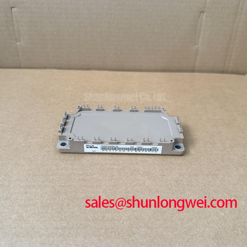
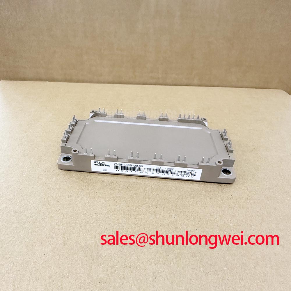
Before fitting the replacement, isolate the drive, inspect the module body and terminals, and verify that the equipment documentation identifies 7MBR35SB120-50 as a Fuji Electric power module rated at 1200 V and 35 A. Record the original terminal wiring, check for visible cracking or discoloration, and compare the DC link, gate drive, braking, and motor connections with the machine schematic.
| Parameter | Specification | Classification |
|---|---|---|
| Manufacturer | Fuji Electric | Official product identification |
| Model | 7MBR35SB120-50 | Official product identification |
| Rated voltage | 1200.0 V | Official datasheet specification |
| Rated current | 35.0 A | Official datasheet specification |
| Package | Module | Official product structure data |
The available factory data confirms the principal electrical ratings and module package. It does not, by itself, confirm the complete pin assignment, switching limits, gate voltage limits, thermal impedance curves, isolation characteristics, or protection functions. Those values should be taken from the applicable Fuji Electric documentation for the exact production revision before energizing a repaired inverter or robotic axis drive.
Thermal verification should begin with the actual switching profile rather than with the nominal current rating alone. A 35.0 A rating is an official device parameter, but the usable current in an industrial drive depends on conduction loss, switching loss, case temperature, cooling path, modulation pattern, overload duration, and the temperature dependence of the complete power stage. For a light industrial automation axis or multi joint robotic articulator, the acceleration and deceleration sequence can create short heat pulses that are not represented by a steady state motor current measurement.
A transient thermal model can represent the junction to case path as several coupled resistance and capacitance sections. In practical simulation, each pulse of calculated semiconductor loss is convolved with the relevant transient thermal impedance response, then combined with the measured case temperature. This approach is useful for estimating peak junction temperature during repeated acceleration events, but it remains a model. The result should be checked against switching loss assumptions, thermal interface condition, heatsink airflow, and the worst operating duty cycle. A model that uses only a single steady state thermal resistance can miss the thermal memory created by closely spaced overload pulses.
Design Consideration: use the official thermal curves for the exact module revision and avoid treating a simulated peak junction temperature as a guaranteed field limit unless the associated case temperature, mounting condition, coolant or airflow condition, and loss model are all controlled. The system designer should verify the temperature margin with thermocouples, infrared measurements used within their limitations, or an equivalent validated test method while reproducing the real mechanical motion profile.
Mechanical installation affects the thermal network just as strongly as the electrical design. The mounting surface should be clean, flat, and free from burrs that could tilt the baseplate or create local air gaps. Apply the thermal interface material according to its own manufacturer instructions, keep the layer uniform, and use a controlled tightening sequence. Clearance around the power terminals should allow the busbar, cable insulation, and probing equipment to remain separated from adjacent conductive parts under vibration and service conditions.
For troubleshooting, compare case temperature at a repeatable load point, then inspect whether one phase or one switching position is consistently warmer. An abnormal temperature distribution may involve current imbalance, gate timing, thermal interface variation, airflow obstruction, motor cable loading, or a damaged companion device. Confirm the phase currents and switching waveforms before attributing the result to the module itself. The Fuji Electric Power Semiconductor and IPM Modules resource provides the appropriate manufacturer context for reviewing module families and application documentation.
Preventing Spurious Faults: Derating Guidelines and Mismatched Parameter Guidelines for 7MBR35SB120-50
Current derating should be established from the complete inverter operating envelope. The relevant boundary is not simply the motor nameplate current. Engineers should examine DC link variation, regenerative operation, ambient temperature, heatsink temperature, PWM frequency, overload repetition, motor cable capacitance, and the time available for fault detection. The 1200.0 V voltage rating should be compared with the measured switching overshoot and regenerative transients at the module terminals, not only with the nominal DC bus value.
Parallel semiconductor paths require both static and dynamic analysis. The positive temperature coefficient commonly associated with IGBT saturation voltage can support static current sharing because the warmer path tends to develop a higher conduction voltage. This is a Design Consideration, not a substitute for measurement, and it does not automatically correct dynamic imbalance during turn on or turn off. Differences in gate resistance, driver propagation delay, emitter inductance, busbar geometry, and thermal coupling can still force one path to switch earlier or carry a disproportionate transient current.
Gate driver sourcing and sinking capability should be selected from the required gate charge, switching speed, gate resistance, isolation behavior, and fault turn off strategy documented for the complete design. A driver with inadequate sink capability can leave the gate vulnerable to Miller induced voltage during the opposite switch transition. A driver with excessive peak current can increase ringing and electromagnetic interference if the gate loop is not compact and damped. The correct balance must be established on the bench with a suitable differential probe and a current probe where practical.
External gate resistance is a tuning component rather than a universal fixed prescription. Begin with the gate network specified by the design documentation, then adjust damping only after observing turn on overshoot, turn off ringing, switching loss, and fault response. Any change should be made symmetrically across equivalent switching positions. Gate resistor placement should be close to the module gate terminal and its intended emitter reference, while the isolated driver return should not share a long path with the high current power return.
When the module is used in an inverter feeding a robotic axis, review the freewheel path and reverse recovery behavior of the associated diode network. A hard reverse recovery event can raise commutation overshoot and increase radiated EMI, especially when the DC link and motor cable form a low damping loop. Designers should evaluate diode reverse recovery softness, busbar inductance, snubber behavior, and conducted emissions together. The related 6MBI450U-120A-05 can be reviewed as a neutral example of a related high power semiconductor module for front end or auxiliary topology analysis, subject to voltage, current, thermal, and control compatibility.
💡 Pro Tip: Keep the commutation path physically symmetrical and verify peak voltage, gate voltage, and phase current with double pulse or representative machine testing before approving the repaired assembly.
Benchtop Waveform Tuning: Mitigating Stress via PCB Gate Loop Layout Symmetry on 7MBR35SB120-50
Waveform tuning should start with a known safe low energy test condition and a measurement setup that does not add excessive loop area. A long oscilloscope ground lead can display ringing that is partly created by the probe connection, while an unsuitable probe reference can expose the instrument to unacceptable common mode voltage. Use an appropriate isolated or differential measurement method and compare the gate to its actual emitter reference at the module terminals.
The auxiliary emitter or driver reference should follow the connection defined by the exact Fuji Electric application documentation. The purpose of a separate low noise control return is to prevent the gate driver from sensing voltage developed by the main emitter current path. If the control return is routed through a shared high current copper section, the voltage produced by di/dt can appear as false gate feedback. That coupling can produce uneven switching, apparent gate oscillation, or a protection trip that is difficult to reproduce at low load.
PCB and busbar geometry should minimize the area of the gate drive loop and keep the outgoing gate path close to its return path. Avoid routing sensitive gate traces beside fast DC link edges for long distances. Where the mechanical construction requires a transition from PCB to module, keep the paired conductors short and secure them against vibration. The power loop and gate loop should be considered separate electromagnetic structures even when they occupy the same assembly.
Long motor cables introduce another measurement and protection issue. The cable can behave as a transmission structure, causing reflected voltage at the motor terminals and additional stress at the inverter output. The resulting peak can approach a multiple of the local switching edge voltage under unfavorable impedance conditions, so the system engineer should verify the motor terminal waveform rather than relying only on the inverter terminal measurement. Cable routing, output filtering, switching edge control, motor insulation capability, and grounding must be evaluated as a system.
During field diagnosis, compare all three phase gate waveforms under the same operating command and then compare the corresponding collector emitter behavior. A mismatch may originate in the driver supply, isolation channel, gate resistor, connector, auxiliary emitter path, probe reference, or module connection. Check the signal path from controller output through the isolated driver to the module before replacing additional power components. This avoids treating a protection symptom as proof of a single failed semiconductor junction.
7MBR35SB120-50 Operational Boundaries: Evaluating Dynamic Gate Impedance Control for Robust Limits
High common mode transients can couple through the isolation barrier and the parasitic capacitances of the power assembly. In a multi axis drive, simultaneous switching and long motor cables can make this condition more severe. The isolated gate driver should therefore be evaluated for its common mode transient immunity in the actual layout, including the isolation barrier, auxiliary supply, connector arrangement, shield termination, and control board return paths. A driver data sheet value alone does not validate the completed inverter.
An active Miller clamp can reduce unwanted gate movement when the opposite switch changes state, provided that the clamp is connected to the intended emitter reference and becomes effective within the required switching sequence. Its usefulness depends on driver timing, gate impedance, parasitic inductance, gate charge, and the voltage transition imposed by the complementary device. Designers should verify the clamp behavior with a high bandwidth measurement setup during the fastest credible commutation event.
A negative off state gate bias may be considered when the driver and the exact module documentation support it. The selected value must remain within the specified gate emitter limits and must account for driver tolerance, start up sequencing, isolation supply behavior, fault turn off, and possible negative transients at the emitter reference. The system designer, rather than a product page, must determine whether a negative bias is appropriate after testing the complete gate loop. Do not apply a negative bias solely because it is common in another IGBT platform.
Dead time is also system determined. Excessive dead time can increase diode conduction and reverse recovery stress, while insufficient dead time can permit cross conduction during propagation delay variation and transient gate disturbance. Establish the timing from measured driver delay, temperature drift, device switching behavior, and the protection response required by the inverter. Verify it at the highest relevant DC link condition and with the motor cable and load connected.
Fast semiconductor fuses and short circuit protection should be coordinated with the module’s documented short circuit capability and the system interrupt path. The fuse I2t must be assessed against the energy that can pass before the electronic protection removes the gate command, while recognizing that a dead short can develop faster than a conventional control loop. No fuse rating or clearing time should be inferred from the 35.0 A continuous rating alone. The complete protection chain should be validated with the manufacturer’s limits, controlled fault testing, and appropriate containment measures.
For alternative evaluation, the 7MBR35UA120 may be reviewed as a related Fuji Electric module reference, but its electrical configuration, terminal arrangement, thermal data, switching behavior, and control requirements must be checked independently before any substitution decision. For broader topology work involving 1200 V silicon carbide technology, the article The 1200 V CoolSiC™ MOSFET Advantage in Three Phase Power Conversion offers a separate technical comparison context rather than a direct replacement instruction.
Safety Interlock Note: Remove all DC link energy and confirm the measured bus voltage has fallen to a safe level before disconnecting the module, gate cable, or oscilloscope connections.