



Content last revised on September 10, 2026
Atmospheric Neutron Radiation Impact on 1200V/1700V Silicon Reliability
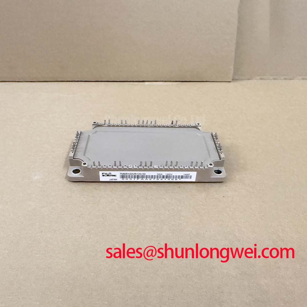
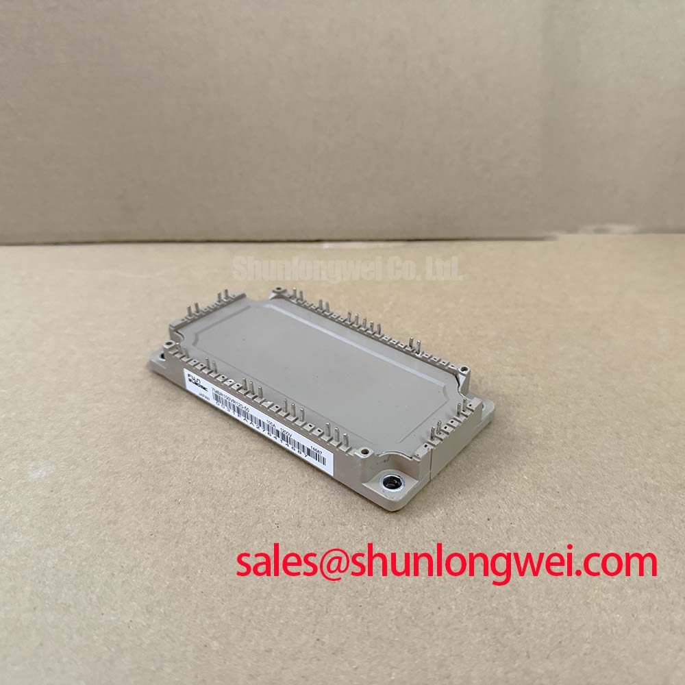
In high-dynamics multi-axis CNC machines and robotic servo drives operating in industrial facilities situated at elevations exceeding 2000 meters, terrestrial cosmic ray neutron flux increases failure rates in high-voltage silicon. High-energy atmospheric neutrons colliding with the silicon lattice of the 7MBR100VR120-50 power integrated module (PIM) can trigger localized avalanche multiplication, leading to catastrophic Single Event Burnout (SEB). For power stages rated at an inverter collector-emitter voltage of VCES = 1200 V (Official Datasheet Specification), the failure-in-time (FIT) rate increases exponentially as the continuous operating DC-bus voltage approaches the rated breakdown limit.
Field data indicates that running a continuous DC link above 800 V at high altitudes drastically elevates SEB susceptibility. To ensure high reliability across multi-axis servo installations, the steady-state DC bus should be engineered with adequate derating headroom, typically maintained between 560 V and 750 V under nominal grid conditions. When troubleshooting unexplained inverter breakdown on high-altitude factory floors where no prior thermal overstress or mechanical short circuit is evident, field engineers must assess voltage stress levels and creepage integrity in accordance with Dielectric Strength and High-Voltage Breakdown Testing standards. Further diagnostic procedures for isolating non-thermal junction ruptures are detailed in the Field Engineer’s Handbook.
| Module Sub-Circuit | Key Parameter | Symbol | Specification Value | Unit |
|---|---|---|---|---|
| Inverter (IGBT) | Collector-Emitter Voltage | VCES | 1200 | V |
| Brake Chopper (IGBT) | Collector-Emitter Voltage | VCES | 1200 | V |
| Converter (Diode Bridge) | Repetitive Peak Reverse Voltage | VRRM | 1600 | V |
| Integrated Thermistor | Internal NTC Resistance (T = 25°C) | R | 5000 | Ω |
Dynamic Braking Chopper Operation & Regenerative Deceleration Energy Absorption
High-speed robotic tool positioning and multi-axis servo reversal demand rapid kinetic energy dissipation. The integrated dynamic braking chopper inside the 7MBR100VR120-50 incorporates an internal brake IGBT rated at VCES = 1200 V (Official Datasheet Specification) designed to switch an external power ballast resistor across the intermediate DC circuit. During hard deceleration cycles, regenerated motor energy pumps up the DC link voltage. If the ballast resistor impedance is selected too low, peak collector current will breach safe operating limits; conversely, high busbar stray inductance (Lσ) causes high-frequency voltage spikes during brake turn-off.
When the chopper switches off high inductive fault currents, the induced collector-emitter voltage overshoot obeys the fundamental relation where peak voltage equals the instantaneous DC link voltage plus the product of total loop stray inductance and turn-off current slew rate. In fast emergency-stop events, parasitic busbar inductance must be minimized using low-inductance laminated busbars and high-frequency polypropylene film snubber capacitors placed directly across the P and N power terminals. For decentralized servo architectures requiring external discrete chopper stages or six-pack configurations without integrated braking switches, engineers frequently evaluate alternative layouts like the 7MBI100U4E-120-50 to balance power density against thermal dissipation requirements.
💡 Pro Tip: During bench troubleshooting of an overvoltage fault trip on a servo drive, verify the health of the internal brake transistor using a digital multimeter in diode-check mode. Measure forward drop across the brake collector and emitter terminals (typically 0.35 V to 0.55 V on the anti-parallel freewheeling path). A continuous reading below 0.05 V confirms a shorted brake silicon die caused by prolonged regenerative overcurrent or improper chopper duty-cycle programming.
PCB Gate Loop Layout Symmetry & Kelvin Emitter Routing Optimization
Rapid switching dynamics in servo inverters generate high current rise rates across the low-side and high-side power loops. Without a dedicated Kelvin emitter connection, the high load current flowing through the module emitter terminal induces a counter-electromotive force across the internal wire-bond parasitic inductance. This induced voltage subtracts directly from the gate-emitter control voltage applied by the driver, slowing down switching transitions, escalating turn-on losses, and triggering gate oscillations.
The 7MBR100VR120-50 separates auxiliary Kelvin emitter terminals from the main power return paths. Gate drive circuits must route the gate command trace and the dedicated Kelvin auxiliary emitter return as a tightly coupled, differential strip-line directly to the driver IC output stages. This minimizes mutual inductive coupling and eliminates parasitic gate loop pickup during high dV/dt cross-talk events. Furthermore, integrating active Miller clamp circuits or maintaining a bipolar gate drive supply (+15 V / -8 V) prevents parasitic capacitive turn-on when the complementary IGBT in the same half-bridge leg turns on rapidly. Circuit designers can explore baseline switching dynamic concepts and cell configurations via Fuji Electric High-Speed Discrete IGBTs.
Transient Thermal Impedance (Z_th(j-c)) & Multi-Layer Foster/Cauer Modeling
Servo applications subject power modules to severe thermal cycling due to repetitive acceleration bursts, tool engagement, and rapid braking cycles. Under heavy pulsed overload conditions lasting under 100 milliseconds, heat does not immediately reach the heatsink; instead, it is absorbed by the thermal capacitance of the silicon die, the solder layer, and the direct copper bonded (DCB) ceramic substrate. Evaluating peak junction temperature (Tj) margins requires dynamic multi-RC thermal modeling using Foster or Cauer impedance networks based on the junction-to-case transient thermal impedance characteristics.
The input stage features a three-phase converter bridge with a rated repetitive peak reverse voltage of VRRM = 1600 V (Official Datasheet Specification), which manages line voltage transients while feeding smooth direct current to the inverter DC bus. Real-time baseplate monitoring is enabled by the integrated negative temperature coefficient (NTC) thermistor exhibiting a nominal resistance of 5000 Ω at 25°C (Official Datasheet Specification). The drive control algorithm uses this sensor to throttle output current during sustained machining overloads before the IGBT silicon reaches its absolute maximum junction operating limit.
⚠️ Field Alert: Never reuse dried thermal interface material when replacing a blown module. Clean the heatsink surface using technical-grade isopropyl alcohol, checking that heatsink flatness is within 50 μm over a 100 mm span. Apply a uniform 80 μm to 100 μm layer of high-conductivity thermal paste using a calibrated screen printer or roller. Fasten the module mounting screws using a calibrated torque wrench in a crosswise pattern: first tighten to a preliminary snug torque of 1.0 N·m, followed by a final tightening torque within 2.5 to 3.5 N·m (Design Consideration for M5 mounting screws). Uneven mounting torque cracks internal ceramic isolation substrates, leading to instantaneous ground faults upon high-voltage bus energization.