


Content last revised on September 10, 2026
PCB Symmetry Considerations for Dual IGBT Half-Bridge Switching Paths
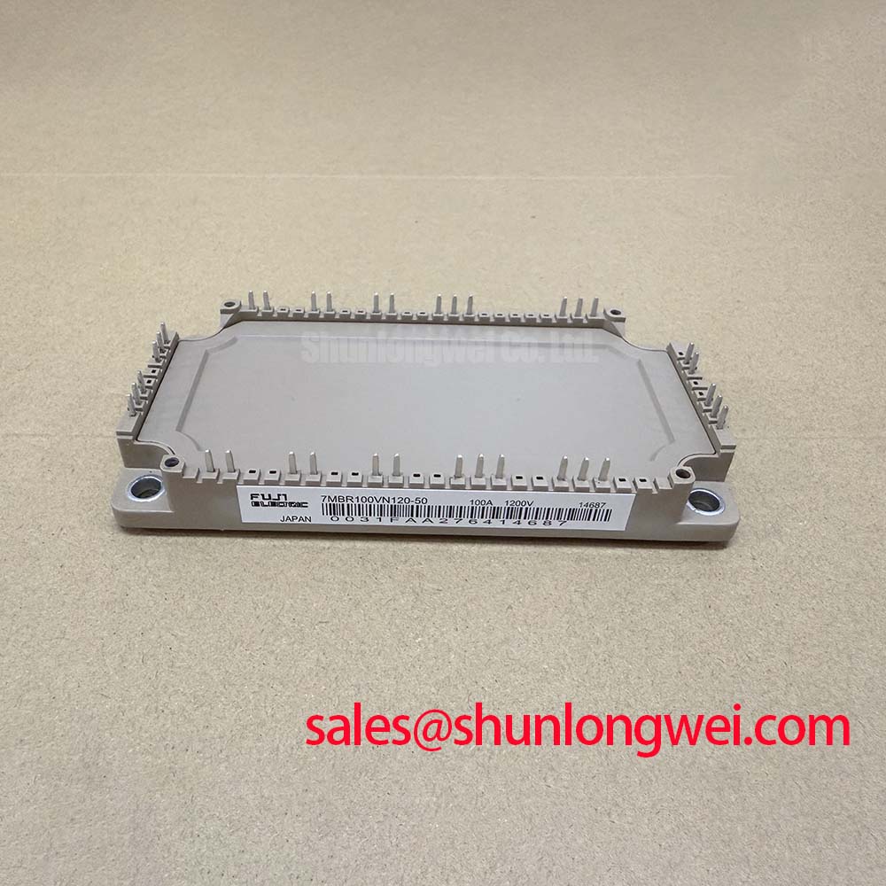
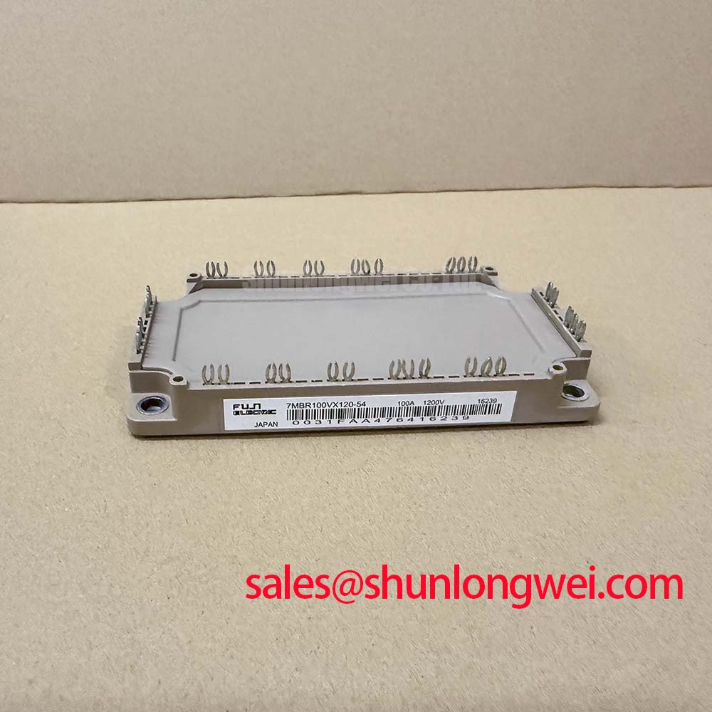
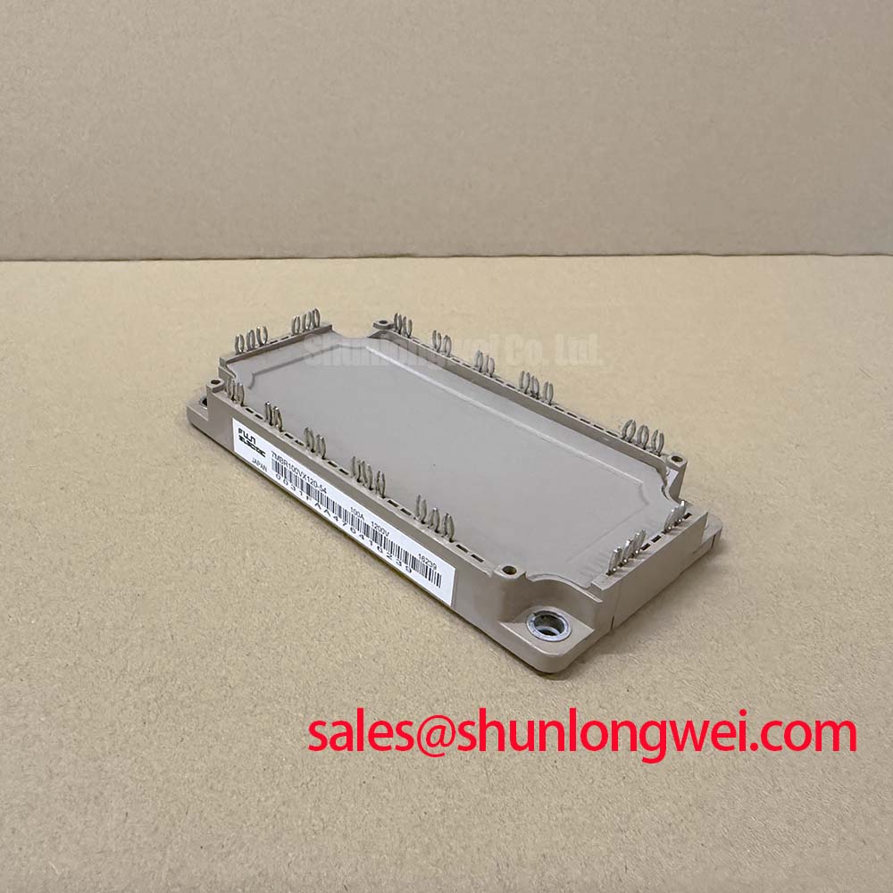
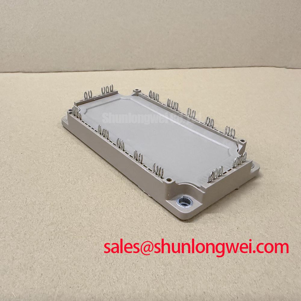
In high-capacity commercial string inverters and micro-grid battery storage systems, maintaining trace symmetry across switching legs is a foundational layout requirement. The 7MBR100VX120-54 integrates a full three-phase inverter, converter, and dynamic braking chopper into a unified Power Integrated Module (PIM) architecture. Rated at a maximum collector-emitter voltage of 1200V (Official Datasheet Specification) with a continuous collector current capability of 100A at a case temperature of 80°C (Official Datasheet Specification), fast turn-on and turn-off transients induce substantial rate-of-current changes across PCB copper runs.
When routing the upper and lower gate-drive channels, the auxiliary Kelvin emitter terminal must remain strictly isolated from the high-current power emitter copper path. Coupling the high-current output loop into the auxiliary gate return introduces a shared parasitic source inductance. During rapid turn-off, this inductive drop acts as negative feedback that counteracts gate discharge, prolonging switching intervals and multiplying turn-off switching losses. Field troubleshooting on inverter assemblies frequently reveals asymmetric gate ringing caused by mismatched return path lengths between Phase U, Phase V, and Phase W legs.
To preserve signal integrity and suppress common-mode noise injection, implement tightly coupled stripline or differential-style paired routing between each gate output and its corresponding Kelvin return. Minimizing the physical loop area formed by the gate-drive path directly limits susceptibility to electromagnetic field pickup emitted by adjacent high-voltage busbars. When retrofitting or evaluating hardware upgrades from older module generations, such as comparing operational pin footprints with the 7MBI100U4E-120-50, verify the auxiliary pin assignments carefully, as gate-emitter layout differences between U-series and V-series platforms dictate trace re-routing to prevent parasitic cross-talk.
Isolated DC-DC Power Supply Sizing for High-Side Floating Gate Drivers
Driving the high-side IGBT switches in string inverters operating off a nominal 800V to 1000V DC bus requires isolated auxiliary bias rails capable of handling extreme voltage slewing. The integrated structure of the 7MBR100VX120-54 is tested for an isolation voltage of AC 2500V for 1 minute (Official Datasheet Specification), protecting control logic from high-voltage transients. However, the external gate driver power supplies must provide reinforced galvanic isolation and exhibit common-mode transient immunity exceeding 100kV/μs (Design Consideration) to prevent false gate triggering during fast bridge commutations.
Calculating the required steady-state output power for each high-side isolated DC-DC converter requires evaluating total gate charge over the targeted switching frequency. For an IGBT operating at a switching frequency of 16kHz with an asymmetric gate drive voltage window from -8V to +15V, the DC-DC converter must continuously supply the charge currents without suffering voltage dips that could pull the device into its linear desaturation region. Using low-capacitance isolated transformer designs limits parasitic displacement currents from migrating into primary-side digital signal processor references.
Freewheeling diode recovery characteristics also influence driver stability. The internal diode paths of the module feature a repetitive peak reverse voltage rating of 1200V and an average forward current rating of 100A (Official Datasheet Specification). When paired with auxiliary switching blocks, engineers reviewing discrete switching dynamics often analyze standard diode recoveries against the performance benchmarks defined in Fuji Electric High-Speed Discrete IGBTs. If complex multi-level topologies or secondary boost stages incorporate dual-pack half-bridges like the 2MBI150-060, ensure that high-side power supply sizing matches the aggregated gate charge load across both stages to prevent thermal overstress on auxiliary regulator chips.
High dv/dt Cross-Conduction Shoot-Through Mitigation via Dedicated Miller Clamps
High voltage transients exceeding 10kV/μs (Design Consideration) are commonplace in commercial energy storage conversion systems during hard switching. When the lower IGBT turns on, the rapid voltage rise across the collector-emitter terminals of the complementary high-side device causes a displacement current to flow through its internal gate-collector parasitic capacitance (Miller capacitance). This current flows back through the external turn-off gate resistor, elevating the gate voltage above the turn-on threshold and causing cross-conduction shoot-through across the DC link.
To eliminate shoot-through risks without incurring excessive turn-off losses, field engineering best practices mandate the implementation of dedicated active Miller clamp circuits alongside negative gate turn-off biasing (-5V to -10V, Typical Starting Point). An active Miller clamp monitors the gate voltage during the turn-off cycle; once the gate drops below approximately 2.0V relative to the emitter, an internal low-impedance MOSFET clamps the gate directly to the negative rail, creating a low-resistance path that bypasses the turn-off resistor.
Desaturation detection circuits (DESAT) must also be configured to safeguard the short-circuit Safe Operating Area (SCSOA). During an output line-to-line fault or grounding failure in a string inverter, collector-emitter saturation voltage climbs rapidly. The DESAT sensing circuit must initiate a soft turn-off sequence within a defined short-circuit withstand window, preventing destructive overvoltage spikes caused by parasitic loop inductance during emergency shutdown.
⚠️ Field Alert: When replacing or re-mounting the 7MBR100VX120-54 onto cold plates or forced-air heatsinks, strictly observe mechanical mounting torque specifications. Uneven bolt tightening leads to ceramic substrate cracking or localized thermal isolation. Apply a uniform 50μm to 80μm layer of high-performance thermal grease (Design Consideration) and torque mounting screws sequentially in cross-diagonal stages to between 2.5 N·m and 3.5 N·m (General Industry Design Consideration for standard M5 module mounting hardware). Over-torquing can permanently warp the copper baseplate.
Junction-to-Case Thermal Network Simulation under High-Pulsed Overloads
Micro-grid applications expose power conversion stages to severe transient current surges during grid synchronization, motor startup, or sudden battery pack discharge. Managing thermal excursions within the module is essential for operational longevity. The inverter section of the 7MBR100VX120-54 features a junction-to-case thermal resistance of 0.17 °C/W per IGBT element (Official Datasheet Specification), with a maximum operating junction temperature rating of +150°C (Official Datasheet Specification).
Evaluating peak junction temperature during heavy overload cycles requires modeling the transient thermal impedance using multi-order Foster or Cauer RC networks. Under short-duration surge conditions (e.g., 10ms to 100ms grid-support burst injection), the thermal capacity of the internal silicon die and direct-bonded copper (DBC) substrate absorbs the thermal pulse before heat conducts into the heatsink mass. Field calculations must account for the junction temperature margin at maximum ambient installation limits.
| Parameter | Datasheet Rating / Status | Operating Target / Consideration | Engineering Note |
|---|---|---|---|
| Collector-Emitter Voltage (VCES) | 1200V (Official Specification) | 650V - 850V DC Bus | Ensures margin against turn-off overshoot spikes |
| Continuous Collector Current (IC) | 100A @ Tc=80°C (Official Specification) | 60A - 75A RMS Steady-State | De-rated for continuous thermal stability |
| Maximum Junction Temperature (Tj) | +150°C (Official Specification) | ≤ +125°C Continuous Run | Extends bond-wire and solder fatigue life |
| Thermal Resistance (Rth(j-c)) | 0.17 °C/W (Official Specification) | Grease layer: ≤ 80μm | Per 1/6 module inverter IGBT channel |
| Isolation Voltage (Viso) | AC 2500V, 1 min (Official Specification) | Functional Reinforced Boundary | Validates safety isolation between baseplate and pins |
High-altitude commercial installations (elevations exceeding 2000 meters) also require cosmic ray-induced single-event burnout (SEB) derating assessments. Operating the DC link at sustained voltages close to the 1200V breakdown ceiling exponentially increases the failure-in-time (FIT) rate due to atmospheric neutron flux. Detailed bench testing procedures, diode drop verification techniques, and failure analysis methodologies are systematically documented in the Field Engineer’s Handbook for technicians conducting site forensics.