Content last revised on September 20, 2026
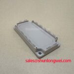
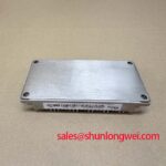
Transient Dynamics & Electrical Design: High-Frequency Commutation Loop Inductance on 7MBR100VN120-50
During commissioning, capture collector-emitter voltage and phase current at the module terminals with measurement methods appropriate to the converter voltage. A waveform that appears acceptable at a distant DC-link measurement point can conceal overshoot at the local commutation path. The electrical mechanism is straightforward: the turn-off peak combines the DC-link voltage with the parasitic loop inductance multiplied by the current-change rate. The actual peak must remain within the 1200 V collector-emitter rating, with the acceptable operating margin determined and proven by the system engineer.
Design Consideration: Keep the DC-link capacitor connection, power terminals, and return path physically compact and geometrically coupled to minimize commutation-loop inductance. A symmetrical planar busbar arrangement can reduce unequal current paths between parallel conductors and help control turn-off overshoot. Layout clearance, creepage, enclosure contamination conditions, and busbar insulation requirements remain system-specific and should be assessed against the equipment’s applicable standards.
When a repaired inverter shows intermittent overvoltage trips, do not attribute the event solely to the power module. Check whether DC-link capacitors remain electrically close to the switching bridge, whether laminated conductors have been reassembled in their original order, and whether a snubber network has changed value or connection integrity. Snubber capacitance and damping must be selected from measured ringing frequency, energy, and temperature behavior rather than copied from another converter revision.
💡 Pro Tip: Preserve symmetrical positive and negative DC-bus routing during service work, then validate turn-off voltage peaks with double-pulse or equivalent switching tests before returning the converter to duty.
The manufacturer’s published semiconductor information can provide wider context on switching-device behavior, while the installed module’s original documentation remains the controlling source for pin allocation, dynamic characteristics, and protection limits. See Fuji Electric High-Speed Discrete IGBTs for related power-semiconductor technical context.
Field Diagnostics & Commissioning: Managing High-C-Rate Battery Cycling Swing in 7MBR100VN120-50 Topologies
In a micro-grid energy-storage converter, the power stage can experience repeated directional changes as battery racks absorb energy and later support the DC link. In four-quadrant operation, both the switching devices and their free-wheel paths participate in changing current conditions. The 1.65 V typical FWD forward voltage at 100 A is an Official Datasheet Specification for the stated test condition, but it is not a complete loss model for a particular switching frequency, junction temperature, or modulation method.
Before commissioning, verify that each gate-drive channel is referenced to the intended power-emitter return and that isolation barriers, driver supplies, command signals, and fault feedback have continuity consistent with the original control design. Gate ringing can arise from common-emitter inductance, long gate connections, altered connector routing, driver-output impedance, or an unsuitable external gate resistor. It can lead to uncertain switching timing or false protection activity, so oscilloscope verification should compare gate-emitter voltage, collector-emitter voltage, and load current on a known-good channel where available.
Engineering Recommendation: Select external gate damping through controlled bench testing, balancing switching loss, voltage overshoot, current ringing, and the driver’s source and sink capability. The gate driver must deliver and remove charge fast enough for the intended switching duty, but its peak current capability and resistor values are system-determined rather than module ratings supplied here. Dead-time control also requires validation because excessive dead time changes free-wheel conduction, while insufficient dead time can permit unwanted overlap conduction.
A load step that causes an alarm may be associated with battery-side current demand, DC-link movement, control-loop response, gate-driver desaturation behavior, cooling limitations, or a combination of these conditions. Record the event state before changing hardware. Useful evidence includes command state, current direction, DC-link voltage, gate waveform, heatsink temperature, fault-latch source, and the timing relationship between them.
For gate-loop measurement practices, timing interpretation, and validation concepts, the technical resource Precision Gate Drive Design provides relevant background. It should be used alongside the equipment schematic and original module documentation, not as a substitute for converter-specific testing.
Where a service bill of materials permits a cross-model evaluation, the 6MBI100L-060 can be reviewed as a separate Fuji Electric module reference. Electrical rating, internal topology, terminal arrangement, gate-drive requirements, thermal interface, control logic, and mechanical fit must all be compared with the original equipment requirements before any substitution decision.
7MBR100VN120-50 Thermal-Electrical Optimization: Evaluating Thermal Capacitance vs Heat Sink Practical Tuning
Inspect the cooling interface before interpreting a thermal fault. Remove old interface material only in accordance with the equipment service procedure, check the mounting plane for debris or damage, and confirm that the heatsink, fan path, coolant circuit, and temperature-sensor connection are functioning as intended. A module can remain electrically functional at low load while showing unacceptable junction-temperature movement during recurring power pulses if heat extraction has degraded.
The inverter IGBT junction-to-case thermal resistance is specified as 0.23 K/W. This Official Datasheet Specification describes the thermal path from junction to case under the stated datasheet methodology; it does not include thermal interface material, heatsink resistance, airflow, coolant performance, mounting pressure, or enclosure temperature. Those external paths determine the actual junction-to-ambient result in the assembled converter.
Design Consideration: Evaluate pulse loading using the manufacturer’s transient thermal impedance information from the applicable module documentation, usually represented by a multi-section thermal model. In practical analysis, instantaneous semiconductor loss is translated through the time-dependent junction-to-case response, then combined with the measured case or heatsink condition. The resulting calculated junction temperature must be checked against the +150°C maximum specified junction temperature, while recognizing that switching and conduction losses depend on the complete operating waveform.
For service diagnostics, compare thermal behavior during equivalent controlled operating states rather than relying on a single external temperature reading. A rising case temperature may indicate insufficient cooling capacity, whereas a relatively stable case with fast protection activity can suggest a local interface issue, altered switching loss, or an inaccurate sensor path. These observations are diagnostic leads, not standalone proof of a particular cause.
Thermal capacitance affects how quickly the junction responds to pulsed loss, while the heatsink governs longer-duration heat removal. Engineers should test both short load pulses and sustained load conditions because the same thermal assembly can behave differently in each time domain. Any mounting-force guidance must come from the module drawing and the host equipment documentation; no mounting torque or interface thickness is stated here as an Official Datasheet Specification for this model.
Preventing Spurious Faults: Fault-Clearing Dynamics: Type-I/II Desatur Guidelines for 7MBR100VN120-50
Before enabling PWM after a repair, verify that the fault-clear path, driver disable path, controller interlock, and emergency shutdown state follow the original converter sequence. Desaturation monitoring is commonly used to identify abnormal collector-emitter voltage during commanded conduction. Its threshold, blanking period, filtering, and response time are properties of the gate-driver and converter protection design, not published official specifications in the parameter set for the 7MBR100VN120-50.
Type-I and Type-II desaturation terminology can describe different protection classifications in controller documentation. The practical requirement is to determine exactly how the installed driver distinguishes a transient switching event from a sustained abnormal conduction condition. Probe the desaturation sensing path with appropriate high-voltage safety controls and confirm that its blanking network, diode path, isolation interface, and fault reporting remain intact. A false trip may reflect sensing noise, ground-reference disturbance, a damaged passive component, or a real power-stage abnormality.
Engineering Recommendation: Use a coordinated soft-turn-off strategy when the host driver supports it, so that a detected fault does not create an unnecessarily abrupt current interruption and associated inductive voltage excursion. The two-stage turn-off profile, clamping method, fault-latch behavior, and restart policy must be chosen by the converter designer and verified against measured collector-emitter voltage, current, and DC-link conditions.
Do not repeatedly reset a latched fault without waveform evidence. First establish whether the event occurs under no-load PWM, controlled resistive loading, a directional battery-power transition, or only after thermal stabilization. Review controller logs where available and compare all bridge legs under equivalent conditions. This approach helps separate a control or sensing anomaly from a commutation, cooling, or load-path issue while retaining the 1200 V, 100 A, and +150°C official boundaries as the core device-level reference points.