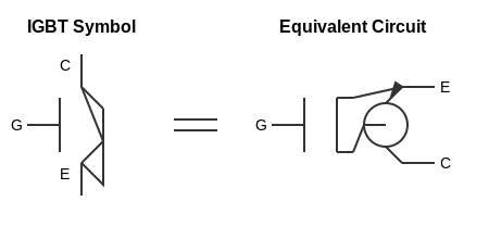
In the demanding world of high-power electronics, engineers constantly seek the ideal switch—a component that is both easy to control and capable of handling immense electrical loads efficiently. The Insulated Gate Bipolar Transistor, or IGBT, emerged as a groundbreaking solution, ingeniously engineered to combine the most desirable traits of two other fundamental components: the MOSFET and the Bipolar Junction Transistor (BJT).
The design philosophy behind the IGBT is to harness the best of both worlds. It integrates the voltage-controlled, high-input-impedance characteristics of a MOSFET with the high-current handling and low on-state voltage drop of a BJT. This unique fusion creates a three-terminal semiconductor powerhouse that bridges the performance gap between MOSFETs (ideal for high-frequency, low-to-medium power) and BJTs (suited for high-power, lower-frequency applications), offering a superior solution for a vast range of high-power systems.

The Fundamental Structure of an IGBT
An IGBT has three primary terminals: the Collector, the Emitter, and the Gate. The Gate terminal is the key to its ease of use. It features a layer of silicon dioxide insulation, just like a MOSFET, which is why it’s called an “Insulated Gate.” This structure allows the device to be turned on and off by applying a voltage rather than a continuous current, dramatically simplifying the required driver circuitry and minimizing drive power consumption compared to a current-controlled BJT.
Internally, the semiconductor structure of an IGBT is more intricate than that of a MOSFET or BJT. It consists of a four-layer PNPN configuration, effectively creating a hybrid device. Conceptually, you can think of an IGBT as an N-channel MOSFET built on the same silicon die to drive a PNP transistor. However, this clever integration introduces a parasitic thyristor structure. If accidentally triggered, this parasitic element can cause a condition known as “latch-up,” where the device gets stuck in the “on” state and can only be turned off by interrupting the current, often leading to device failure. To prevent this, designers incorporate features like a resistive short between the base and emitter of the parasitic NPN transistor, a testament to the careful engineering required to ensure reliability.
A Closer Look at Gate Design: Planar vs. Trench
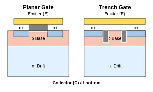
The physical layout of the gate has a significant impact on the IGBT’s performance. Two primary structures have evolved over time:
Planar Gate
The original and more straightforward design, the planar gate structure sits on the surface of the semiconductor, above the n+ emitter and p-base regions. While effective, this layout introduces a parasitic JFET-like effect within the device’s current path. This effect adds resistance when the IGBT is conducting, resulting in a higher on-state voltage drop (VCE(sat)) and increased power loss.
Trench Gate
A more advanced and efficient design, the trench gate is etched vertically into the silicon, extending through the n+ emitter and p-base regions. This vertical orientation completely eliminates the parasitic JFET effect seen in planar designs. The result is a significantly lower on-state voltage requirement, which directly translates to reduced conduction losses and higher overall efficiency. The development of trench gate technology marks a key evolution, transforming the IGBT from a simple hybrid into a highly optimized power switching device.

Vertical Structure: Punch-Through (PT) vs. Non-Punch-Through (NPT)
The performance of an IGBT is also heavily influenced by the thickness and doping of its internal layers, leading to two main vertical structure types:
Punch-Through (PT) IGBT
PT IGBTs utilize a heavily doped p+ collector/anode region and a thin n- drift region. This design includes an additional n+ “buffer” layer, which helps to rapidly deplete charge carriers during turn-off, reducing switching losses. The primary advantage of the PT structure is a lower on-state voltage. Thin-wafer PT technology further optimizes this by using extremely thin layers for both the drift region and the collector, enhancing performance even more.
Non-Punch-Through (NPT) IGBT
In contrast, NPT IGBTs feature a thicker, lightly doped n- drift region and a more lightly doped p+ collector. This structure prevents the electric field from “punching through” to the collector during the off-state. NPT IGBTs generally exhibit faster switching speeds and have lower switching losses, particularly at low to medium currents. However, their on-state voltage can be higher than that of PT devices, especially under high current conditions.
Summary of IGBT Structural Characteristics
| Characteristic | Sub-Type | Structural Features | Performance Impact |
|---|---|---|---|
| Gate Type | Planar Gate | Gate is located on top of the n+ emitter/buffer and p-base regions. | Introduces a JFET-like effect, causing a higher on-state voltage drop. |
| Trench Gate | Gate extends vertically through the n+ emitter/buffer and p-base regions. | No JFET effect, significantly reducing on-state voltage for higher efficiency. | |
| Vertical Structure | Punch-Through (PT) | Features a heavily doped p+ collector/anode and an n+ buffer layer. | Lower on-state voltage but can have higher switching losses; optimized with thin-wafer tech. |
| Non-Punch-Through (NPT) | Uses a thicker, lightly doped drift layer and a thinner, lightly doped collector. | Typically faster switching and lower losses at medium currents; on-state voltage can be higher. |
Conclusion: An Evolving and Optimized Powerhouse
The structural complexity of the IGBT is not an accident; it is the direct result of decades of engineering focused on balancing performance, efficiency, and reliability. The hybrid nature of the IGBT delivers the core benefits of simple voltage control and robust current handling, but it is the continuous innovation in gate and vertical structures that truly unlocks its potential. As detailed in research from institutions like the IEEE, the trade-offs between designs like PT and NPT allow for application-specific optimization.
By refining these internal architectures, manufacturers can minimize parasitic effects like latch-up, reduce on-state voltage, and increase switching speeds. This means that modern IGBTs are far more than simple hybrids; they are highly sophisticated components tailored for specific applications, from the high-frequency demands of solar inverters and electric vehicle powertrains to the raw power requirements of industrial motor drives and welding equipment.
Understanding these structural nuances is key to selecting the right component. This knowledge allows engineers and designers to make informed decisions, matching the specific performance characteristics of a Trench Gate NPT or a Planar Gate PT IGBT to their application’s unique demands. For your next high-power project, explore the wide range of advanced IGBTs available at SLW-ELE.COM to find the perfect, highly optimized solution.
