

Content last revised on September 26, 2026
1MBI600V-120 Operational Boundaries: Transmission Line Impedance Mismatch
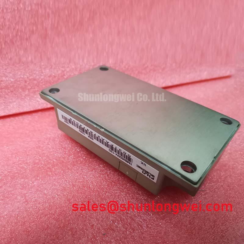
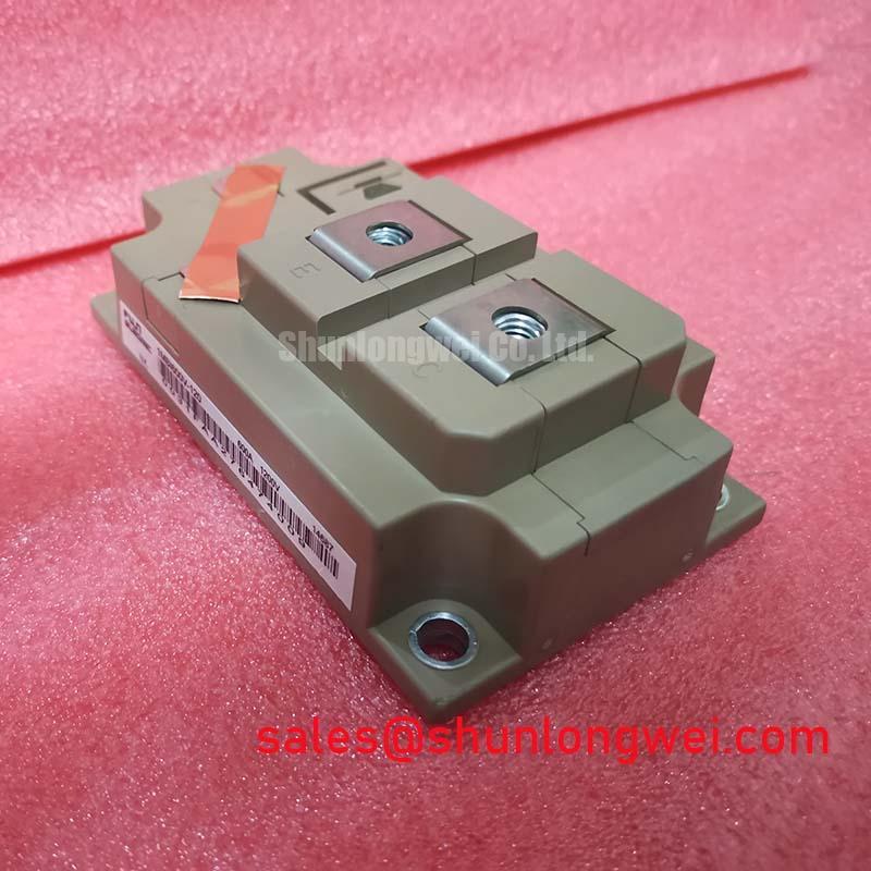
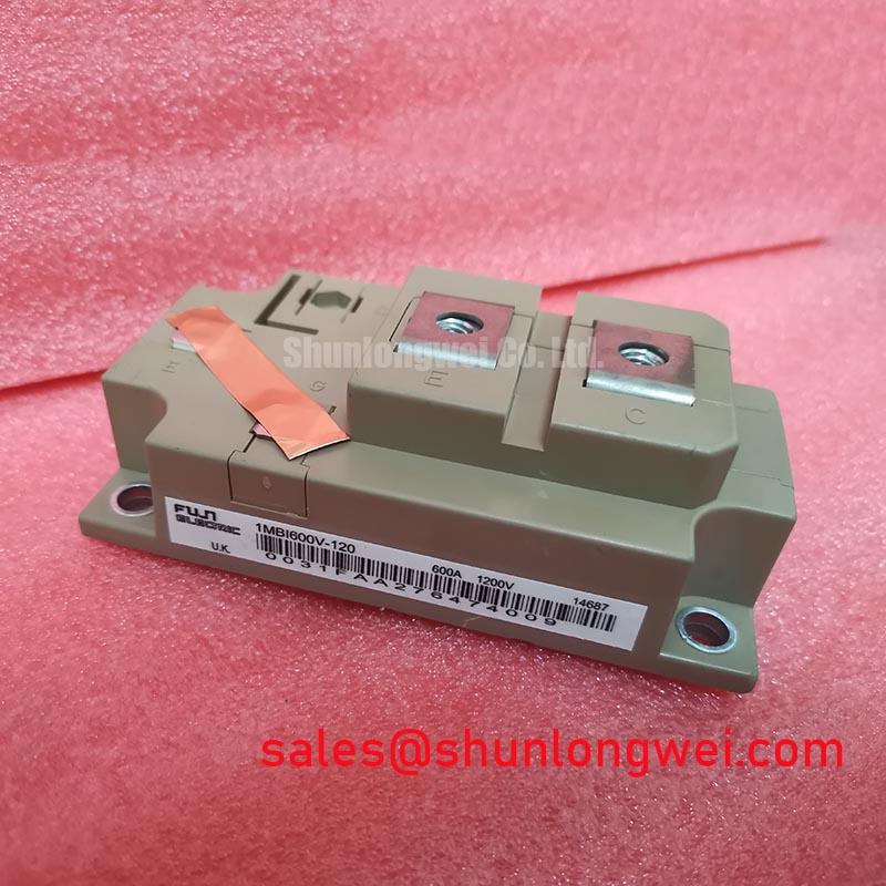
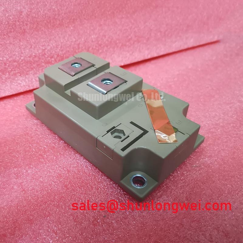
With the DC bus isolated and discharged, first verify that the installed module nameplate matches the required 1MBI600V-120 rating before reconnecting gate drive and power terminals. This Fuji Electric unit is specified at 600 V and 1200 A in a Fuji Power Module housing, which establishes the electrical identity that must be checked against the original inverter documentation.
| Parameter | Official Specification |
|---|---|
| Manufacturer | Fuji Electric |
| Part Number | 1MBI600V-120 |
| Collector Emitter Voltage | 600 V |
| Rated Current | 1200 A |
| Package | Fuji Power Module |
Long motor or output leads can behave as transmission lines during fast switching edges. Under an impedance mismatch, reflected voltage can raise the terminal stress significantly and, in some installations, approach twice the DC bus voltage. This is a Design Consideration, not an official voltage transient rating for this module. Engineers should measure collector emitter waveforms at the power terminals with suitable differential instrumentation and compare peak values against the 600 V official rating.
For inverter welder or medium frequency induction heating equipment, output chokes and dv dt filters are commonly evaluated when cable routing, transformer leakage inductance, or load leads create oscillation. Keep high current conductors short, closely coupled, and physically separated from gate control wiring. If ringing appears only after a cable replacement or layout repair, inspect lead routing, output filter connections, grounding continuity, and the original power stage configuration before changing gate drive settings.
For a lower current Fuji Electric module in a different voltage class, the 3MBI50SX-120-02 can be reviewed as a separate engineering reference. Its electrical, thermal, mechanical, and driver interface requirements must be checked independently rather than treated as a direct replacement.
1MBI600V-120 Operational Boundaries: Evaluating Regenerative DC Bus Voltage Surge Limits
During rapid load deceleration, stored mechanical or magnetic energy can return to the DC bus and raise its voltage. In induction heating power supplies, this condition can also occur during abrupt load changes, control interruption, or resonant tank transitions. The 1MBI600V-120 should therefore be assessed within the complete DC bus arrangement, including capacitors, braking path, protective sensing, and the switching sequence defined by the original equipment designer.
A braking IGBT and ballast resistor are often used to convert returned energy into heat, but their ratings must be selected from the system energy profile, duty cycle, resistor thermal capacity, and control threshold. This is an Engineering Recommendation: record DC bus behavior during deceleration and abnormal stop testing, then verify that the installed braking circuit responds consistently without exceeding the module’s official 600 V boundary.
Freewheel diode reverse recovery can contribute to current commutation stress and radiated noise. Snubber networks may reduce ringing when their capacitance, resistance, placement, and thermal duty are validated on the actual converter. Avoid treating a snubber fitted to another power stage as automatically suitable. Gate drive dead time also requires confirmation at the installed switching conditions so that complementary devices do not conduct simultaneously.
Semiconductor fuses should be evaluated from their published time current and I²t characteristics together with the converter’s prospective fault energy. A fuse is part of coordinated fault protection, not a substitute for gate drive desaturation protection, DC bus sensing, or correctly sequenced shutdown logic.
1MBI600V-120 Thermal Electrical Optimization: Isolation Interface Integrity and Practical Tuning
Before commissioning after a module replacement, inspect the heatsink surface for flatness, corrosion, old thermal compound residue, and blocked airflow paths. Apply thermal interface material as a thin, continuous layer according to the equipment service procedure, then tighten terminals and mounting hardware in the specified sequence. The official parameters supplied for this part identify its voltage, current, and package, but do not establish a reinforced isolation rating or a common mode transient immunity value. The system integrator should verify those requirements from the original driver, isolation component, and equipment documentation.
Gate driver isolation, power supply isolation, creepage spacing, and control cable routing should be checked as an assembly. A spurious gate pulse can originate from common mode coupling, incorrect gate return routing, contamination, moisture, or a damaged driver channel. Use oscilloscope measurements referenced to the known good gate drive path to determine whether a disturbance appears at the driver output, module gate terminal, or power loop.
Where parallel semiconductor paths are used in a converter, static and dynamic current sharing should be verified through matched layout, matched drive timing, and thermal observation. Positive temperature coefficient behavior can support static sharing in some operating regions, yet it does not remove the need to examine switching imbalance. Consult Fuji Electric’s power semiconductor and IPM resources and Fuji Electric Europe semiconductor information for broader product family context.
⚠️ Maintenance Note: Regularly monitor terminal contact temperature and confirm that cooling air passages remain clear after filter cleaning or enclosure service.
Field Diagnostics and Commissioning: DC Bus Low Inductance Busbar Design in 1MBI600V-120 Topologies
At turn off, the observed collector emitter peak is influenced by DC bus voltage plus the voltage created by stray loop inductance and the rate of current change. This engineering relationship means that a compact laminated busbar, close DC link capacitor placement, and symmetrical current paths can help suppress overshoot. The required inductance target, capacitor value, and clamp arrangement must be determined through switching tests on the actual inverter rather than adopted as fixed values.
When diagnosing a repaired power stage, begin with passive checks of busbar fasteners, capacitor terminals, module connections, gate return paths, and cooling hardware. Then commission at controlled operating conditions while observing DC bus ripple, gate waveforms, collector emitter switching behavior, and temperature rise. A waveform change after maintenance may indicate altered conductor geometry, degraded capacitor performance, grounding issues, or a driver timing problem; it should be investigated as a system interaction rather than assigned to one cause.
For structured review of power loop design, switching stress, protection coordination, and thermal reliability, see the Power Electronics Masterclass. This module should remain evaluated against the original equipment circuit, cooling arrangement, and documented service limits.