




Content last revised on September 18, 2026
MCC162-18IO1 Circuit Protection & Reliability: Calibrating High-Frequency Switching Loss Dissipation
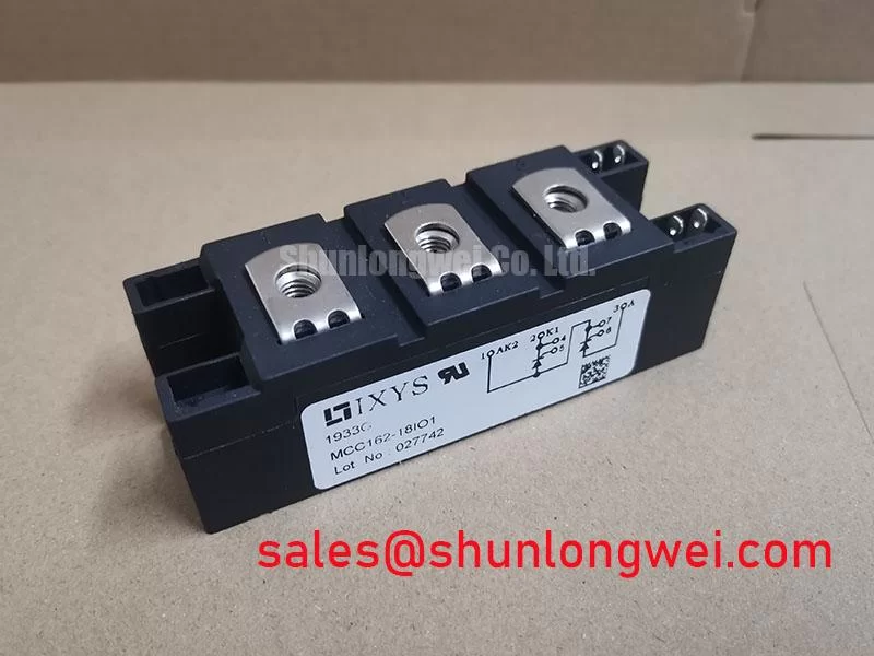
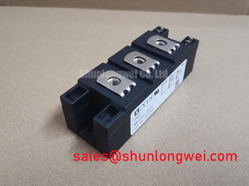
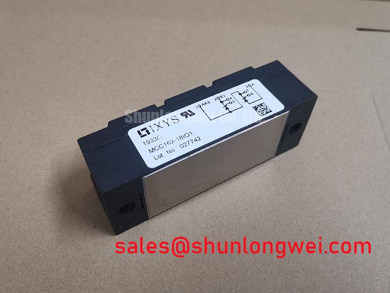
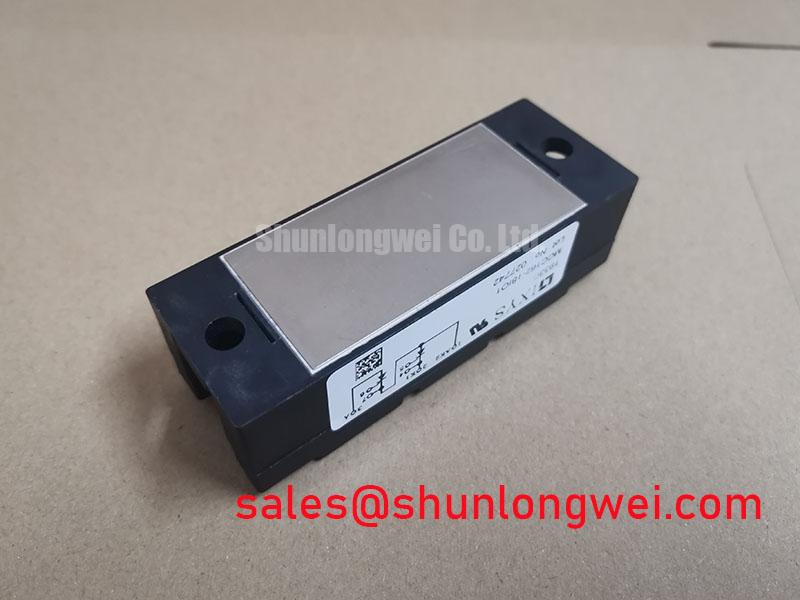
Before energizing a replacement assembly, verify the nameplate boundary of MCC162-18IO1 against the controller bill of materials, then check that each power terminal is isolated from the heatsink and that the firing leads match the original circuit drawing. This IXYS dual thyristor module is officially rated at 1800 V and 162 A, supplied in a module package. Those ratings define the device identity; they do not by themselves establish suitability for a complete converter, capacitor-switching cabinet, or static var compensator installation.
For maintenance assessment, record the incoming supply characteristics, connected load, protective fuse part number, firing-board revision, and heatsink condition before removing the original module. A controlled thyristor circuit can show similar external symptoms when its trigger path, snubber network, current path, or cooling interface has changed. Comparative measurements against the documented circuit and an approved test method provide a more reliable basis for repair decisions than a single continuity result.
| Parameter | Official Specification |
|---|---|
| Manufacturer | IXYS |
| Product model | MCC162-18IO1 |
| Product type | Dual thyristor module |
| Rated voltage | 1800 V |
| Rated current | 162 A |
| Package | Module |
The 1800 V rating is an Official Specification for MCC162-18IO1 and should be checked against the maximum repetitive electrical stress observed in the actual topology. In a thyristor-switched capacitor stage or grid-tied static var compensator, the relevant voltage exposure is affected by source conditions, capacitor-bank state, circuit inductance, commutation conditions, and transient suppression performance. The system engineer should capture representative waveforms at the installed operating points and verify the measured peak conditions against the applicable device and system limits.
Protection coordination begins with the actual protection documentation. A semiconductor fuse selected for the branch must be evaluated using the fuse manufacturer's time-current and I2t information together with the converter's prospective fault current, upstream protection, conductor capability, and thyristor module documentation. The official voltage and current ratings of MCC162-18IO1 are not a substitute for an I2t coordination study. Where a fuse table or device-specific surge-current data is required, use the approved source for the installed design rather than transferring values from another module family.
Reverse recovery in an associated diode path deserves attention because it can shape commutation current, conducted noise, and radiated emissions. Parameters such as reverse-recovery peak current, reverse-recovery time, and recovery softness must come from the relevant diode datasheet or measured switching test. They are not stated by the supplied official identification data for MCC162-18IO1 and should not be assumed. A sharp recovery event can coincide with a changing thyristor current path, while a different recovery characteristic may alter ringing and switching stress without necessarily indicating a module fault.
Design Consideration: keep the commutation loop physically compact and preserve the original busbar geometry when replacing a module. This supports control of parasitic inductance during current transfer and lets the commissioning engineer compare switching behavior with the known circuit baseline. The principles behind resonant and soft-switching current transitions are described in Zero Voltage Switching Resonant Converter Topologies, although the operating behavior of an installed thyristor circuit must still be assessed from its own topology and waveforms.
Inspect the terminal hardware for looseness, overheated plating, displaced lugs, damaged insulation, and evidence that a conductor has been pulled sideways during service. A terminal connection with added resistance can contribute to local heating and unstable current sharing, but the finding should be confirmed by inspection and appropriately controlled electrical testing. Do not alter terminal arrangement solely to create a tidier cable route if that change increases the area of the high-current loop.
Safety Interlock Note: Isolate, lock out, and verify the discharge state of every connected capacitor bank before touching module terminals or firing connections.
Transient Dynamics & Electrical Design: Dynamic Firing Delay Angle Adjustment on MCC162-18IO1
For phase-controlled AC-to-DC equipment, firing delay angle is a system control variable rather than an inherent MCC162-18IO1 setting. Across a broad firing-angle range, including commands from near zero toward 150 degrees where the installed control scheme permits it, the average conversion behavior, displacement power factor, source current waveform, and reactive-power demand can all change. The resulting current duty must be verified at the module location, especially during capacitor switching, command transitions, and abnormal-grid recovery sequences.
The dual thyristor arrangement should be checked against the actual schematic before firing leads are connected. Confirm the designated anode, cathode, and gate relationships from the controlled-equipment documentation and the applicable IXYS datasheet. A wiring diagram copied from a visually similar package is insufficient because terminal conventions and circuit arrangements can differ. Cold checks can help identify an obvious shorted power path or an unintended connection to the mounting assembly, but they do not prove trigger sensitivity, latching behavior, dynamic blocking capability, or high-current performance.
Gate-drive pulse width, pulse repetition, trigger timing reference, isolation method, and gate-cathode return routing are system-determined. Engineering Recommendation: compare trigger waveforms at the module terminals with those from a verified operating channel, using suitably rated isolated instrumentation. This helps distinguish timing mismatch, inadequate firing energy, noise coupled into the reference path, and an upstream control issue. The firing circuit must remain within the device manufacturer's applicable gate limits, which should be taken from the original product documentation rather than inferred from the 162 A current rating.
In static var compensator and thyristor-switched capacitor equipment, a firing-angle adjustment can affect more than one branch. Assess phase balance, capacitor stage state, controller interlocks, and source synchronization before attributing abnormal reactive-power response to the module. The Shindengen power semiconductor module and diode reference provides useful industry context on power semiconductor assemblies, while replacement decisions should remain tied to the ratings, topology, and mechanical interface of the installed IXYS part.
When the repair documentation calls for a compatible device review, PD104VT2T1 can be examined as a separate candidate. Compatibility requires confirmation of voltage class, current duty, terminal arrangement, triggering requirements, mounting footprint, insulation arrangement, thermal path, and approved circuit behavior. It should not be treated as an automatic substitute for MCC162-18IO1.
Preventing Spurious Faults: Ensuring Uniform Heatsink Contact Pressure Guidelines for MCC162-18IO1
Remove old interface residue from the heatsink with a method compatible with the installed equipment, then inspect the mounting surface for raised debris, corrosion, dents, and localized discoloration. Place MCC162-18IO1 only on a clean, flat interface and follow the applicable manufacturer mounting instructions for the module package. Uniform contact pressure is important because an uneven mechanical interface can create localized thermal resistance even when the external heatsink appears substantial.
The thermal resistance from junction to case, commonly identified as Rth(j-c), must be taken from the official module datasheet when thermal calculations are required. It is not included in the provided official parameter set and must not be estimated as an MCC162-18IO1 factory value. The complete thermal path also includes the case-to-heatsink interface, the heatsink condition, airflow or liquid cooling behavior, enclosure temperature, and the actual conduction and switching losses of the circuit.
Design Consideration: apply thermal interface material according to the equipment and material supplier instructions, with the aim of filling microscopic surface variation without creating an unnecessarily thick layer. Tighten mounting hardware in a balanced sequence so the baseplate settles evenly. The correct torque and fastener requirements must be verified from the specific module mechanical documentation and host equipment procedure; no mounting torque is asserted here as an official MCC162-18IO1 value.
After installation, inspect for a gap between the module and heatsink, cracked housing features, distorted mounting surfaces, displaced insulators, or leads under mechanical tension. Temperature rise can be monitored during a controlled commissioning test, but an elevated reading may reflect several conditions including load profile, airflow restriction, degraded cooling hardware, altered control timing, or contact pressure. Compare the measurement location and operating condition with the maintenance baseline before changing the semiconductor module again.
For equipment teams that maintain both power conversion hardware and operator-interface assemblies, The Ultimate Guide to Industrial TFT LCD Technology is a separate reference for industrial display evaluation. It does not define thermal or electrical limits for MCC162-18IO1; each subsystem requires verification against its own documentation and operating environment.
Assembly Integrity & Layout Architecture: Implementing Turn-On Current Rise Limiting for MCC162-18IO1
Before modifying an RC snubber, series reactor, or capacitor-bank connection, document the existing component values, lead routing, polarity where applicable, and physical placement. These networks influence voltage rate of change, current rise, commutation behavior, and noise coupling. Their final values are determined by the system voltage, source impedance, load characteristics, device behavior, thermal capacity, protection strategy, and measured transient response. MCC162-18IO1 being rated at 1800 V and 162 A does not supply a universal snubber or reactor value.
Engineering Recommendation: preserve short, direct, and symmetric high-current paths around the controlled branch to limit parasitic inductance that can produce unwanted switching overshoot. The commissioning team should validate the resulting peak voltage and current behavior with correctly rated measurement equipment under controlled operating conditions. This is especially relevant after a busbar replacement, capacitor-bank rewiring, or relocation of a suppression component, because a mechanically plausible layout can still alter transient behavior.
A series saturable reactor may be evaluated by the system designer where turn-on current-rise control is required, but its magnetic characteristics, saturation behavior, current duty, and thermal performance must be matched to the real circuit. Likewise, an RC snubber must be evaluated as a network, including resistor pulse capability, capacitor voltage capability, expected dissipation, and connection inductance. A failed snubber part, unstable trigger path, or unexpected source transient can produce similar waveform symptoms; test evidence is required before identifying one as the sole cause.
Review the gate return routing independently from the main power path. Shared impedance between high-current conductors and the trigger reference can introduce unwanted gate-cathode disturbance during commutation. Keep the intended reference path controlled, maintain clearance and insulation practices required by the host equipment, and verify firing behavior through the complete duty sequence. Where an upstream rectifier or related power-semiconductor branch is being reviewed at the same time, PD104SL7 is a related component page that can support a separate specification comparison.
For a grid-tied SVC or thyristor-switched capacitor cabinet, release the assembly only after the power terminals, firing connections, fuse coordination records, heatsink interface, suppression network, and controller interlocks have been checked against the equipment documentation. That procedure keeps the replacement assessment centered on the actual MCC162-18IO1 IXYS dual thyristor module and the electrical conditions it will encounter in service.