

Content last revised on September 13, 2026
7MBR75VZ120-50 Fuji Electric 1200V 75A PIM Power Module
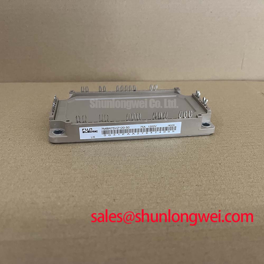
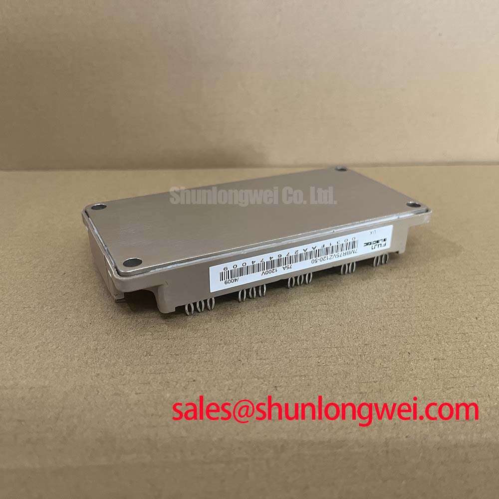
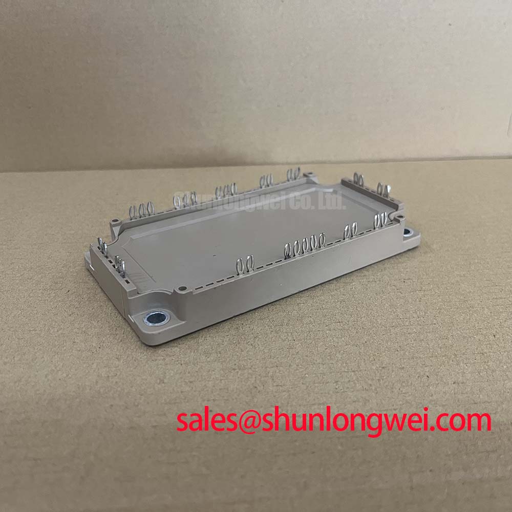
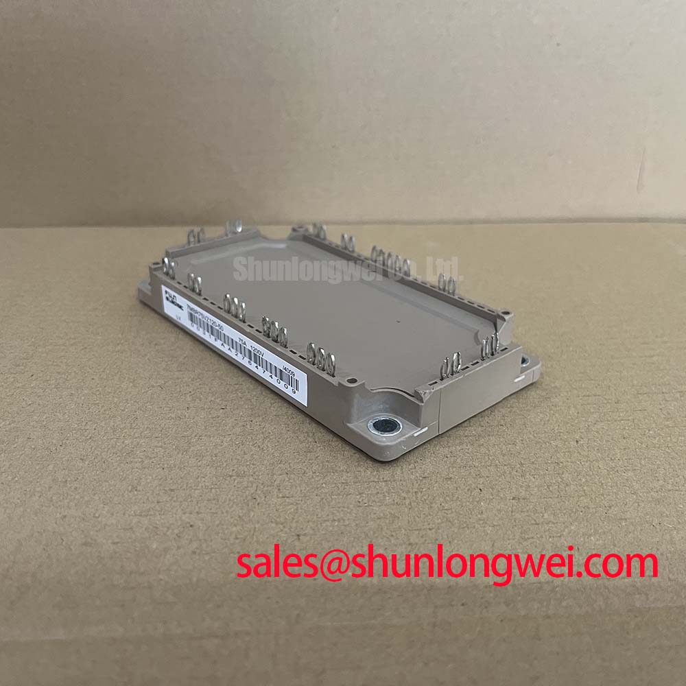
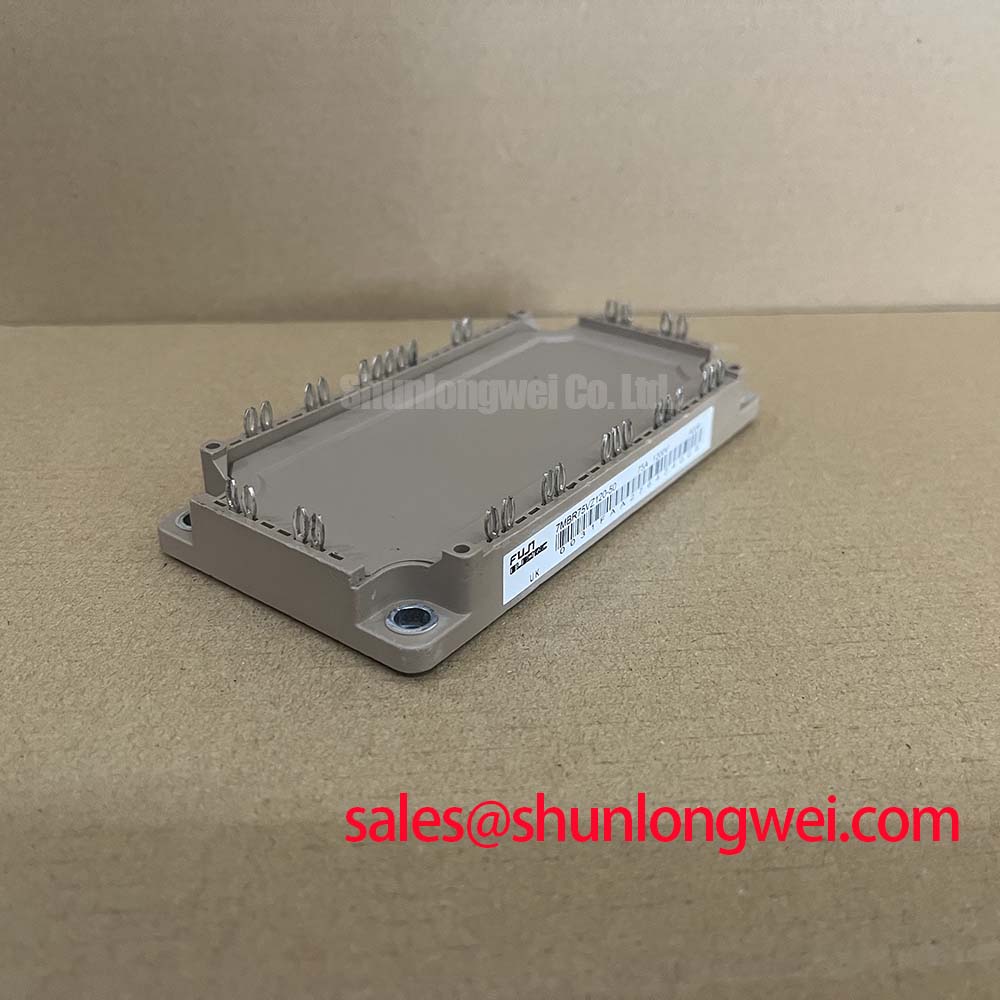
Begin incoming inspection with the module completely isolated: check the printed part number, inspect the case and terminals under good lighting, then verify the intended voltage and current class before connecting it to any test fixture. The 7MBR75VZ120-50 is identified in the supplied product data as a Fuji Electric PIM power module with a rated voltage of 1200.0 V, a rated current of 75.0 A, and a Module package.
| Parameter | Value | Data classification |
|---|---|---|
| Manufacturer | Fuji Electric | Product identification |
| Model | 7MBR75VZ120-50 | Product identification |
| Rated voltage | 1200.0 V | Official Specification |
| Rated current | 75.0 A | Official Specification |
| Package | Module | Official Specification |
| Product category | PIM power module | Catalog classification |
These headline ratings should be treated as device identification data rather than a complete operating envelope. Switching frequency, duty cycle, case temperature, cooling arrangement, gate-drive conditions, overload profile, and the surrounding inverter topology determine the usable operating point. Engineers evaluating this part for a heavy-duty variable frequency AC motor drive should compare the original system documentation and the complete Fuji Electric specification set before energizing the replacement.
For a cold-state bench check, use an isolated digital multimeter and follow the original terminal drawing rather than assuming that a similar-looking module has the same internal connection arrangement. A diode-range reading across the documented power paths can help identify an open circuit, an unexpected short, or an abnormal mismatch between equivalent paths. This is a screening method, not a substitute for a controlled semiconductor curve test. Gate terminals should remain protected from static charge, and the module should not be tested while connected to the control board or DC-link capacitors.
💡 Bench Tip: Keep the device in ESD-safe handling conditions and record cold-state readings against a known-good reference from the same documented configuration before applying any drive signal.
Benchtop Waveform Tuning: Mitigating Stress via Symmetrical Busbar Geometry for High-Current Operation
When the 7MBR75VZ120-50 is evaluated inside a high-current inverter leg, begin with the physical current path rather than the oscilloscope settings. The positive and negative DC-link paths should be arranged to minimize unnecessary loop area, with the switching path kept compact and mechanically supported. Symmetrical busbar geometry is a Design Consideration for reducing unequal stray inductance between parallel or complementary current paths. The final geometry must be verified through switching waveforms, terminal temperature measurements, and peak-voltage checks at the actual operating condition.
Static current sharing benefits from the positive temperature coefficient commonly associated with IGBT on-state voltage, but that general behavior should not be treated as a guaranteed sharing specification for this exact part without the applicable Fuji Electric datasheet. Any parallel arrangement requires matched electrical paths, similar thermal conditions, and independent verification of current balance. Designers should check the voltage observed at the actual power terminals, not only at a remote oscilloscope probe point, because probe-loop inductance can hide or exaggerate switching stress.
Gate-loop wiring deserves the same symmetry as the power path. Keep the forward gate-drive path and return path closely coupled, separate high-current commutation conductors from sensitive gate wiring, and avoid routing the gate return through a shared high-di/dt power trace. If the module provides an auxiliary emitter connection in the original application, the control return should follow the documented terminal arrangement and remain separate from the power-emitter path where the system layout requires it. The existence and exact function of any auxiliary terminal must be confirmed from the original connection diagram.
During troubleshooting, compare turn-on and turn-off waveforms at the same probe locations. Unequal switching delay, a different collector-emitter overshoot, or visible ringing on one path may indicate layout asymmetry, probing error, gate-driver mismatch, or an interaction with the freewheeling path. Change one variable at a time and verify the result with thermal measurements. The 1200.0 V rating and 75.0 A rating are Official Specifications; they do not establish a universal DC-link voltage, switching current, or short-circuit operating time for every drive.
For a repair team reviewing compatible hardware, the 6MBI100S-140 may be evaluated as a separate, objectively specified module. It should not be treated as an automatic substitute. Terminal assignment, electrical ratings, gate-drive requirements, mechanical fit, protection behavior, and thermal performance must all be compared with the original design.
Transient Dynamics and Electrical Design: Suppressing Cres-Induced Gate Voltage Spikes
High dv/dt at the switching node can couple through device capacitances and the surrounding layout, producing an unintended gate-voltage disturbance. Cres is discussed here as a circuit-level parasitic or capacitance-related influence, not as a confirmed standalone parameter of the 7MBR75VZ120-50. A Design Consideration for the gate-drive circuit is to reduce common impedance, keep the gate loop compact, and provide a controlled turn-off path that remains effective during the fastest commutation event.
An active Miller clamp can be considered when the driver architecture supports it. The clamp should be connected according to the driver manufacturer’s timing and current requirements, while the module’s documented gate-emitter limits remain the controlling boundary. A negative gate bias can also be considered in systems where the driver, isolation scheme, and device documentation allow it, but the correct value is system-determined and must be verified through double-pulse testing, gate-emitter monitoring, and fault-condition checks. No negative-bias value should be assumed solely from the module model number.
Bootstrap arrangements require particular attention in a half-bridge drive. The bootstrap capacitor must retain sufficient gate-drive energy during the intended high-side pulse sequence, while the charging diode must recover without creating an unwanted disturbance in the control loop. Engineers should verify the capacitor’s high-frequency impedance, charging path, refresh interval, driver quiescent demand, and gate-charge requirement using the complete switching design. These conditions cannot be established from the supplied 1200.0 V and 75.0 A headline ratings alone.
Freewheeling diode reverse recovery can influence both switching loss and radiated EMI. A softer recovery characteristic generally reduces the abrupt current transition, but the actual result depends on junction temperature, commutation current, DC-link impedance, gate resistance, stray inductance, and the selected switching sequence. If the bench waveform shows a sharp current snap or excessive ringing, inspect the diode commutation loop and snubber placement before changing the gate-drive timing. An RC or RCD snubber is a Design Consideration that requires system-level loss and temperature validation; it is not an inherent specification of this module.
Fuji Electric’s Power Semiconductor and IPM Modules resource and its Power Semiconductors Portal provide useful manufacturer-level context for confirming the relevant device family and documentation. The reseller product page should be used together with the applicable manufacturer documents when gate-drive limits, switching characteristics, or protection functions affect the replacement decision.
Transient Dynamics and Electrical Design: Overvoltage Trip Prevention via Fast-Switching Braking Control
During motor deceleration, the motor can return kinetic energy to the DC link. If the drive cannot transfer or dissipate that energy through its intended braking path, the DC-link voltage may rise until the inverter protection responds. The 7MBR75VZ120-50 should therefore be assessed as one element in the complete drive topology, not as an independent braking-energy solution.
The braking IGBT, its gate driver, the ballast resistor, the DC-link capacitor bank, and the control threshold must be evaluated together. The resistor’s pulse-energy capability and thermal recovery depend on the actual deceleration profile, motor load, duty cycle, and enclosure cooling. Designers should calculate the energy returned during the most demanding permitted stop, then verify the resistor and braking switch with measured DC-link waveforms. The switching device voltage and current ratings supplied for this model do not define the correct braking resistor value or braking threshold.
Use a fast, properly isolated voltage measurement method at the DC link and compare the measured trip behavior with the drive controller’s documented limits. An apparent overvoltage fault may also involve regenerative load changes, capacitor aging, braking-control timing, busbar inductance, or an incorrect feedback signal. Inspect the braking loop for loose connections and excessive conductor length, but avoid assigning a single cause without waveform evidence.
Clearance and creepage around the DC link and braking terminals should follow the applicable equipment insulation design and safety standard. The module package is officially identified as Module, but the supplied data does not provide terminal spacing, isolation voltage, mounting dimensions, or a certified insulation class. Those details must be taken from the applicable Fuji Electric drawing and the drive manufacturer’s construction file. Thermal interface material should be applied as a thin, continuous layer appropriate to the selected heatsink surface; the system builder must determine the assembly method, clamping hardware, and validated mounting torque from the mechanical documentation.
For the upstream portion of the power path, engineers may review the 6MBI450U-120A-05 as an associated module for topology evaluation. This link describes a separate product and does not establish interchangeability with the 7MBR75VZ120-50. Rectifier behavior, DC-link ripple, braking response, and inverter switching should be evaluated as a coordinated system.
Preventing Spurious Faults: Output Sinusoidal Filter versus dv/dt Reactor Guidelines
Before selecting an output filter for a variable frequency AC motor drive, measure the voltage at the motor terminals with a probe and connection method suitable for the switching environment. Long motor cables behave as transmission-line structures, and impedance mismatch can produce reflected-wave overshoot at the motor input. The often-discussed possibility of a terminal peak approaching twice the incident step is a system-level transmission-line concern, not a confirmed performance value for this Fuji Electric module.
A dv/dt reactor, sine-wave filter, or other output network should be selected according to motor insulation requirements, cable length and construction, switching frequency, common-mode behavior, allowable voltage drop, and the drive control method. A reactor reduces the rate of voltage transition but does not necessarily create a sinusoidal motor waveform. A sine-wave filter imposes greater impedance and may affect current regulation, power loss, resonance, and low-speed operation. The system integrator should model and test the complete drive, cable, filter, and motor combination before approving the configuration.
Filter placement is important. Keep the connection between the inverter output and filter physically controlled, route phase conductors together, and avoid placing sensitive feedback or encoder wiring alongside the high dv/dt output conductors. Verify the filter’s voltage, current, thermal, and switching-frequency limits against the real operating envelope. If a fault appears only with a long cable or only after a filter is installed, compare motor-terminal waveforms, common-mode current, and protective-trip records with a known-good cable arrangement.
The 7MBR75VZ120-50 is listed with a 1200.0 V rated voltage, 75.0 A rated current, and Module package. These Official Specifications support initial product identification, while filter selection, braking performance, gate-drive tuning, insulation coordination, and EMC behavior remain application-specific engineering tasks. Additional system-level guidance is available through the Industrial Applications resource.