Content last revised on October 25, 2026
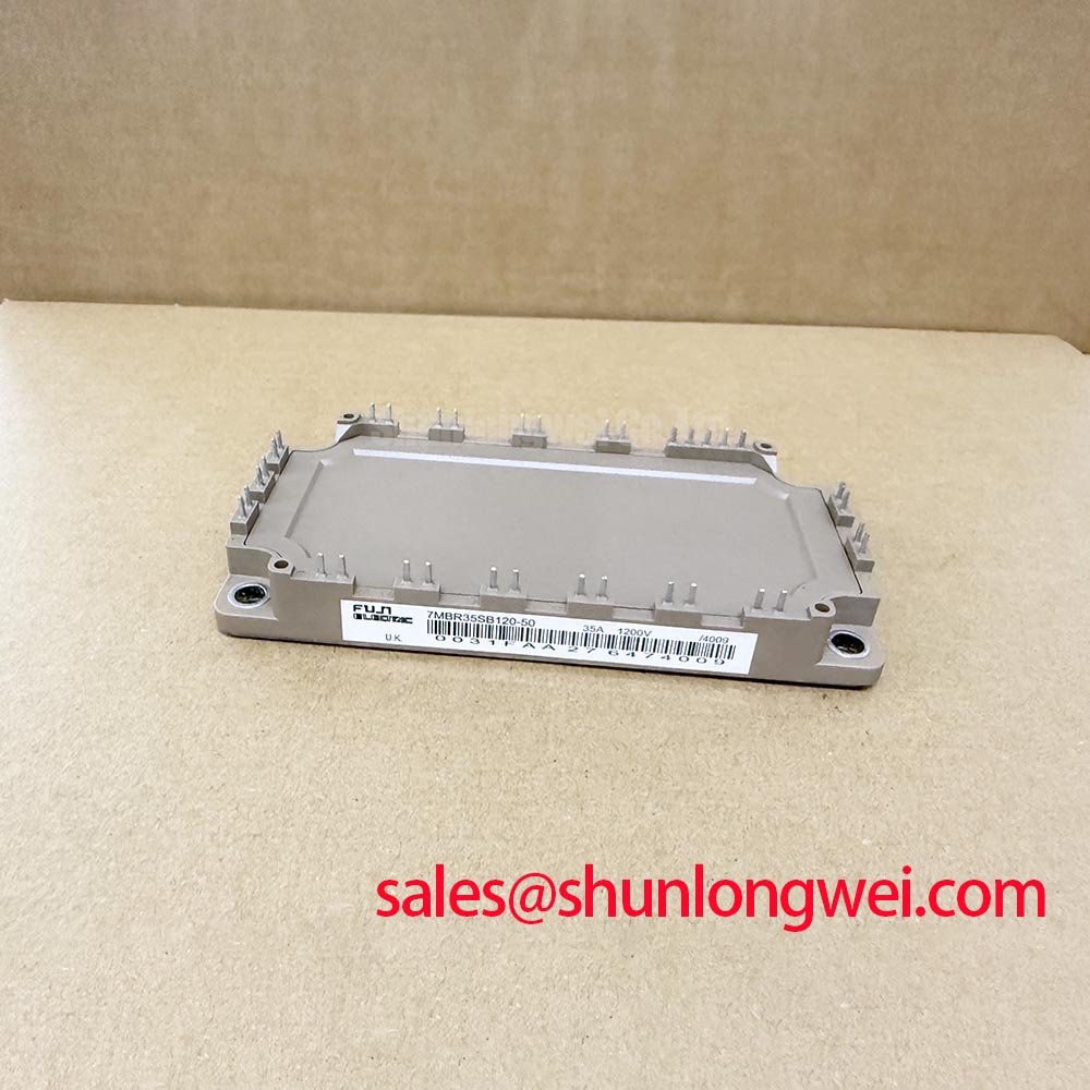
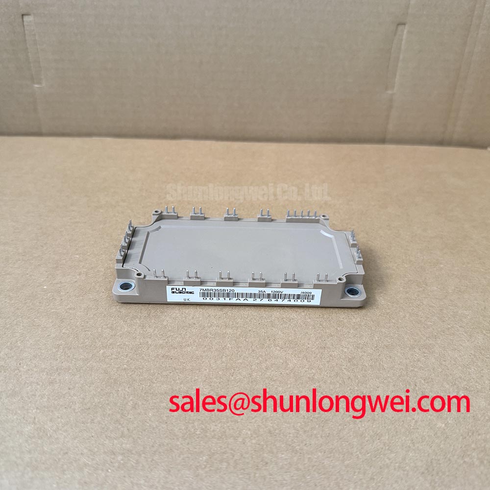
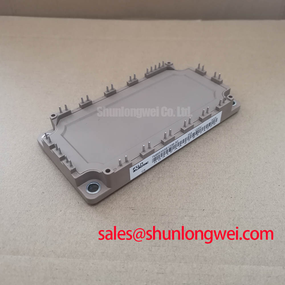
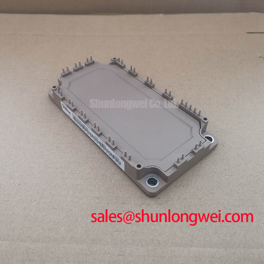
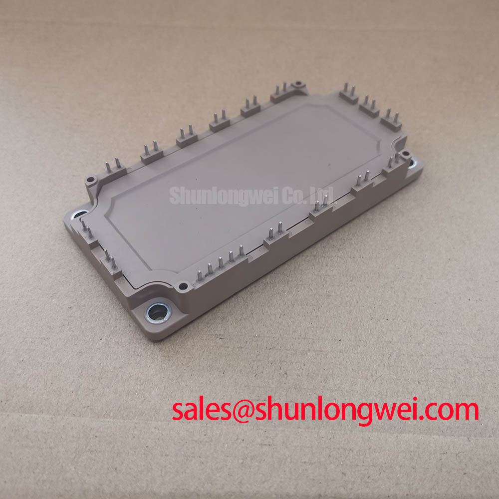
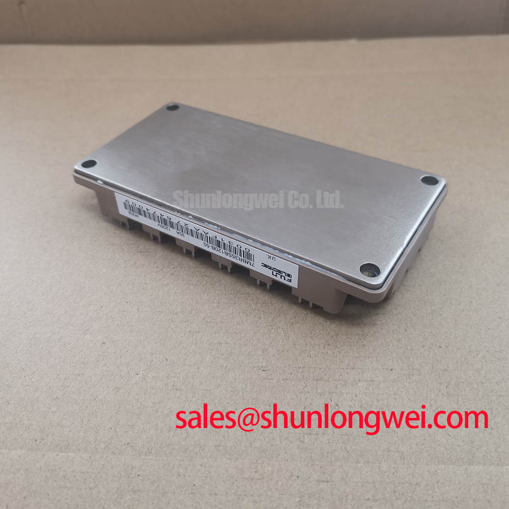
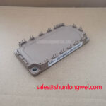
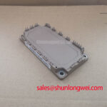
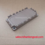
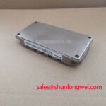
7MBR35SB120B-50 Product Overview
When a precision motion actuator reports an overcurrent or switching fault, isolate the DC link, remove the gate drive connection, and compare the power terminals and emitter return path with a known serviceable assembly before applying test voltage. The 7MBR35SB120B-50 is a Fuji Electric power module specified at 1200.0 V and 35.0 A, with a Fuji Power Module package classification. These are official product specifications for initial replacement screening, not a complete operating limit for an assembled inverter.
For precision stepper and BLDC motor servo actuators, the module should be assessed together with the DC link, gate driver, braking path, current feedback, and thermal interface. A matching voltage and current label does not by itself confirm electrical compatibility. The service engineer should also compare terminal arrangement, gate-drive behavior, isolation requirements, switching frequency, protection timing, heatsink contact, and the original equipment manufacturer’s commissioning limits. Fuji Electric’s Power Semiconductor and IPM Modules resource provides useful manufacturer-level context for power semiconductor integration.
| Parameter | Specification | Engineering meaning |
|---|---|---|
| Manufacturer | Fuji Electric | Use the original equipment documentation to confirm the approved replacement position. |
| Product model | 7MBR35SB120B-50 | Match the complete suffix during procurement and maintenance documentation. |
| Rated voltage | 1200.0 V | Official datasheet specification for voltage-class screening. |
| Rated current | 35.0 A | Official datasheet specification; actual current capability depends on system conditions. |
| Package | Fuji Power Module | Confirm mechanical footprint, terminal layout, insulation arrangement, and heatsink interface before installation. |
| Product category | PIM | Catalog classification for an intelligent or power module category. |
Benchtop Waveform Tuning: Mitigating Stress via PCB Symmetry Considerations for 7MBR35SB120B-50
During bench tuning, first separate the gate-driver return path from the high-current emitter route so the driver does not reference a voltage that moves with load current. A dual-switch power layout can develop emitter mutual coupling when the auxiliary gate return shares copper, vias, or connector pins with the main commutation current. The resulting common impedance can alter the apparent gate voltage and encourage oscillation, uneven turn-off, or unintended turn-on during the opposite switch transition.
Design Consideration: route the auxiliary emitter return directly to the gate-driver reference, while the high-current emitter connection follows the shortest practical power path to the DC-link and load loop. Keep the outgoing and returning power conductors geometrically close where possible, and avoid placing sensitive gate traces alongside the switching node for long parallel distances. The purpose is to reduce shared inductive voltage and capacitive coupling, not to impose a fixed PCB geometry on every inverter.
Symmetry is particularly important when the module is used in a phase-leg or bidirectional converter. The gate path for each switching device should have comparable trace impedance, via structure, and connector treatment. A visibly shorter trace on one channel can produce different propagation and damping behavior, even when both driver outputs are configured identically. Place the driver close to the module terminals, keep the high-current loop compact, and prevent the gate return from passing through a copper region that also carries braking or regenerative current.
For regenerative braking, the switching loop must withstand the transient created when energy is transferred toward the DC link and braking resistor. The module’s 1200.0 V rating is an official voltage classification, while the measured switching peak is determined by bus voltage, commutation rate, stray inductance, snubber behavior, and load condition. Engineers should capture the collector-emitter waveform at the module terminals with a suitable differential probe and verify that the measurement loop itself does not add misleading inductance.
When a waveform shows ringing, alter one physical variable at a time. Inspect the probe ground arrangement, compare the auxiliary emitter reference with the power emitter reference, and then examine gate resistance, driver output impedance, and local decoupling. A ringing waveform may reflect layout coupling, probe error, gate-loop resonance, or a wider commutation problem. The correct corrective action should follow the measured location and timing of the disturbance rather than a single assumed fault.
In a high-power braking stage, laminated busbar construction can reduce the loop area between the positive and negative conductors, but the final arrangement remains system dependent. The design team should evaluate turn-off overshoot at the actual DC-link voltage and load current, then confirm that the semiconductor voltage margin remains acceptable during repeated regenerative events. The linked Industrial Applications reference can support broader maintenance and test planning for demanding power conversion equipment.
For a neutral procurement comparison, the 7MBR50SD120 is a separate Fuji Electric module that may be reviewed when the equipment documentation calls for a different current class. It should not be treated as an automatic substitute. Mechanical fit, terminal assignment, gate characteristics, thermal behavior, protection coordination, and the original drive manufacturer’s approval all require separate checking.
⚠️ Maintenance Note: Clean the heatsink and inspect the thermal interface during scheduled service, then monitor contact temperature and verify that the cooling airflow has not been restricted by dust or cable routing.
Benchtop Waveform Tuning: Mitigating Stress via Short-Circuit Energy Let-Through Matching on 7MBR35SB120B-50
Short-circuit protection must be coordinated as an energy event rather than judged only by the fuse current label. The semiconductor protection fuse has a total clearing I²t characteristic that includes its pre-arcing and clearing behavior, while the power module has a short-circuit withstand capability defined by its own device and gate-drive conditions. The protection study should compare these characteristics on the same basis and under the actual DC-link fault topology.
The fuse selection review should begin with the fault path: DC-link source impedance, busbar inductance, capacitor discharge, cable contribution, and the location of the protective element relative to the module. A fuse that interrupts the external source quickly may not prevent the local capacitor bank from delivering a damaging pulse through the switching device. The test plan should therefore examine both the initial fault current and the energy that remains available while the fuse clears.
For the 7MBR35SB120B-50, the official 1200.0 V voltage rating and 35.0 A current rating identify the device class, but they do not replace the module’s short-circuit waveform limits or the fuse manufacturer’s time-current data. The commissioning engineer should obtain the applicable module short-circuit conditions and compare them with the selected fuse’s total clearing I²t, peak let-through current, interrupting voltage, and installation environment. If the required curves are not aligned, the protection network needs redesign before full-power operation.
Dead-time and gate interlock deserve equal attention. Complementary switches must not receive overlapping turn-on commands while one device is still carrying current or recovering from turn-off. The appropriate dead-time is determined by driver propagation mismatch, gate discharge behavior, temperature, load current, and the measured switching transition. Rather than copying a value from another inverter, observe both gate-emitter signals and the phase-node voltage with isolated measurement equipment during controlled commissioning.
Interlock signals should be routed so that a fault on one driver channel cannot leave the complementary channel permanently enabled. Hardware interlock is preferable for fast shoot-through prevention, while the controller should retain a separate software fault response for desaturation, overcurrent, DC-link abnormality, or driver supply loss. The interlock path should be checked during power-up, reset, emergency stop, and brownout recovery, since unsafe overlap can occur during control-state transitions rather than during normal command operation.
In a bidirectional DC-DC battery converter, repeated charge and discharge cycles place the switching loop, thermal interface, and braking or clamp network under changing stress. Measure the temperature rise at both light and heavy regenerative operation, and compare the cooling response after direction reversal. This helps distinguish a gate-drive timing issue from a thermal accumulation issue. The module should not be assigned a battery duty cycle solely from its nameplate current; the complete converter topology and cooling system determine the practical operating envelope.
For field commissioning, begin with a current-limited DC-link source and a controlled switching command. Confirm that the gate signals remain mutually exclusive, then increase voltage and load in measured stages while recording collector-emitter stress, gate behavior, phase current, and heatsink temperature. If the fuse clears repeatedly during low-energy testing, inspect command overlap, driver supply stability, current-sensor polarity, and the fault latch path before changing the protective fuse rating.
Field Diagnostics & Commissioning: Active Miller Clamp Implementation in 7MBR35SB120B-50 Topologies
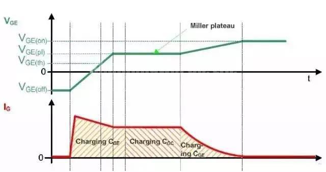
An active Miller clamp is evaluated at the point where a switching device turns off and the opposite switch produces a rapid phase-node transition. The changing collector-gate capacitance can inject current into the off-state gate circuit. If the gate driver return is shared with a noisy emitter path, the resulting gate excursion can reduce the intended off-state margin and contribute to cross-conduction. A dedicated low-impedance clamp path can hold the gate closer to its intended off-state reference during this interval.
The clamp circuit should be placed physically close to the gate and emitter connections used by the driver. Keep the clamp-current loop separate from the power commutation loop, and avoid routing its control signal through the switching-node copper. The driver reference should follow the auxiliary emitter reference selected for the gate circuit, while the power emitter connection should carry load current through the intended high-current path. This arrangement helps the clamp respond to the local gate condition instead of a remote ground potential.
Negative gate bias is a system design option, not an automatic feature that can be assumed from the module part number. If the original drive uses a negative off-state voltage, the integrator should verify the gate-emitter absolute limits, driver supply sequence, clamp threshold, fault behavior, and transient response against the relevant manufacturer documentation. A negative bias that is applied before the driver is ready, or that collapses during a supply fault, can create a different gate-stress condition from the one expected in normal operation.
When diagnosing suspected Miller-induced turn-on, monitor the off-state gate-emitter waveform at the module terminals while simultaneously observing the phase node and collector current. Use a short, low-inductance probe connection appropriate for the measurement equipment. Compare the event with and without the active clamp enabled only under controlled, current-limited conditions. A gate pulse observed at the driver output but not at the module terminal can indicate a connection or measurement issue; a pulse present at both locations requires review of clamp timing, gate-loop impedance, and commutation conditions.
The protection sequence should also be tested during abnormal transitions. Remove the command while current is flowing, interrupt the driver supply in a controlled test, and confirm that the clamp and interlock place both switches in a safe state. Test emergency-stop behavior separately from a normal controller disable because the two paths may have different propagation delays. Designers should verify the peak collector-emitter voltage against the DC-link voltage during switching tests and confirm that the measured result remains acceptable across the intended temperature and load range.
Precision servo actuators can be sensitive to small changes in switching timing because current ripple affects torque smoothness and position response. After gate tuning, check motor current symmetry, regenerative braking behavior, and fault recovery rather than judging the result from the gate waveform alone. If the actuator uses a separate braking resistor or front-end rectifier, inspect its electrical relationship with the inverter DC link. The 7MBP10PE120 can be reviewed as a separate rectifier or complementary power-stage reference when the original system architecture includes that type of front end; it is not an automatic replacement for the subject module.
Before returning equipment to service, inspect the mounting surface, thermal compound condition, terminal tightness, creepage path, connector seating, and enclosure humidity exposure. Condensation, dust accumulation, and deteriorated thermal material can change the electrical and thermal conditions that were present during the original commissioning. Record the measured waveform, heatsink temperature, DC-link condition, and protection response so later maintenance staff can compare changes against a known operating baseline.