

Content last revised on September 25, 2026
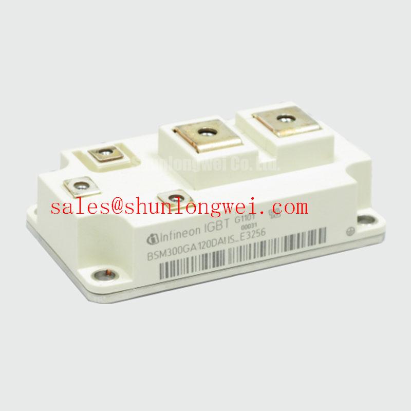
Field Diagnostics & Commissioning: Mitigating Hard Switching Transients in BSM300GB120DLC_E3256 Topologies
For electric material handling and forklift low voltage traction systems, begin commissioning with the DC link isolated and the gate drive disconnected. Confirm that the power terminals, auxiliary terminals, and gate connections correspond to the approved circuit drawing rather than relying on a visual assumption about terminal order. A cold inspection should include case damage, terminal deformation, contamination, loose hardware, and signs of overheating around the busbar interface.
Short circuit protection requires coordination between the gate driver, desaturation or VCE monitoring circuit, current sensing, and the inverter control system. A type I or type II short circuit response may be evaluated with a response target below 10 μs only when this value is supported by the applicable gate driver design, module data, and system test plan. It should not be treated as a confirmed factory rating for this module. The engineer should verify the actual short circuit safe operating area, fault duration, gate resistance, DC link condition, and junction temperature using the relevant Infineon documentation.
Two stage soft turn off is a design consideration for reducing the abrupt current interruption that can produce inductive overvoltage. The first stage should limit the rate of current change while the second stage completes gate discharge under controlled conditions. The appropriate timing and gate voltage are system determined. During bench testing, measure collector emitter voltage directly at the module terminals with a suitable high voltage probe and compare the measured peak with the application’s DC link and insulation limits.
Keep the commutation loop compact and arrange the positive and negative busbars so their magnetic fields oppose where practical. This reduces stray inductance and helps suppress turn off overshoot, but the final result depends on the complete mechanical layout. Check creepage and clearance around the 1200 V circuit after installing covers, insulating barriers, spacers, and service wiring. The Infineon IGBT Modules & Discretes Official Portfolio provides the appropriate manufacturer reference point for device family and application documentation.
BSM300GB120DLC_E3256 Thermal Electrical Optimization: Symmetrical Busbar Geometry for High Current Practical Tuning
At the stated 300.0 A rating, busbar geometry, contact quality, and cooling conditions require verification as part of the complete traction inverter assembly. Do not infer continuous operating capability from the current label alone. The permitted current depends on switching frequency, duty cycle, case temperature, heat sink performance, pulse duration, and the manufacturer’s specified test conditions.
A positive VCE(sat) temperature coefficient can support static current sharing between parallel semiconductor paths because a warmer path may develop a higher conduction voltage. This is a general device behavior consideration, not a guarantee that arbitrary parallel connections will share current correctly. Designers should match conductor impedance, thermal paths, gate loop geometry, and switching timing, then confirm dynamic balance with current probes during representative acceleration, braking, and regenerative charging events.
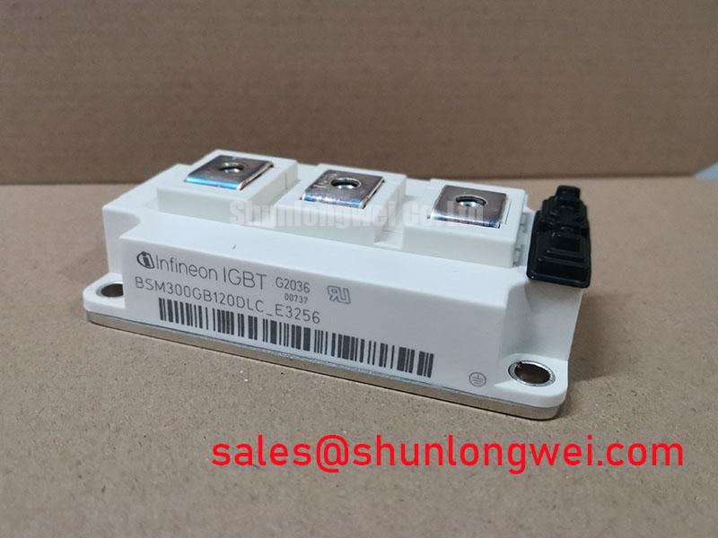
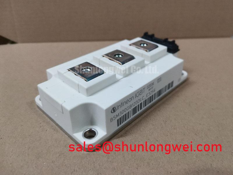
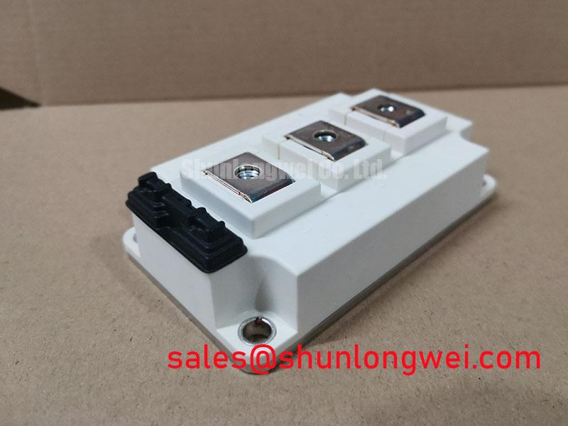
Before energizing the unit, trace each busbar from the DC link through the switching path and confirm polarity against the approved schematic. Inspect contact faces for oxide, uneven seating, and contamination. Vibration resistant fastening should maintain stable contact pressure without distorting the module terminals. Any mounting hardware, torque value, washer arrangement, and locking method should follow the original mechanical documentation or the applicable equipment standard rather than being assumed from the package appearance.
For bidirectional DC DC battery charging and discharging, review thermal cycling at the module baseplate, the busbar joints, and the cooling assembly. Repeated changes in load direction can expose weak contact interfaces and aged thermal materials. A maintenance program should trend contact temperature and inspect the heat sink air path during scheduled service. Maintenance Note: Isolate the DC link and allow the equipment to discharge fully before touching gate, auxiliary, or power terminals.
When a compatible replacement study is required, engineers may compare the electrical and mechanical requirements with the separately listed BSM75GD120DLC, but substitution must be validated against voltage, current, topology, gate drive, cooling, and terminal compatibility rather than selected by family resemblance.
Field Diagnostics & Commissioning: Kelvin Emitter Connection in BSM300GB120DLC_E3256 Topologies
Do not assume that a Kelvin emitter connection is present unless it is identified in the official terminal drawing for the exact device variant. If the documented configuration provides a separate auxiliary emitter return, route the gate driver return to that reference and keep it separate from the high current emitter path. This reduces the influence of emitter mutual inductance and helps the driver observe a cleaner gate emitter voltage during rapid switching.
During troubleshooting, compare the gate emitter waveform at the module terminals with the waveform measured at the driver board. A difference between the two locations may indicate common mode ground bounce, excessive loop inductance, an unsuitable probe connection, or an unintended return path. Use short probe connections and verify the measurement method before changing gate resistance or protection thresholds.
Long motor cables can create transmission line reflections that increase the measured collector emitter stress at the inverter output. Filtering, damping, motor cable selection, and switching edge control should be evaluated as a system. The module rating of 1200.0 V does not by itself establish immunity to every reflected wave or installation transient. Confirm peak voltage at the power terminals under the longest intended cable, highest operating temperature, and regenerative operating condition.
Gate drive isolation, common mode shielding, and controlled return routing are practical design considerations when the traction inverter is installed near battery switching hardware. A negative gate bias must not be assumed for this product unless confirmed by the approved gate drive and module documentation. The final on state and off state gate voltages, desaturation blanking, fault latch behavior, and reset sequence require validation with the selected driver and the complete control system. The The Ultimate IGBT Knowledge Base can provide additional background on switching behavior, parasitic paths, and module integration principles.
Benchtop Waveform Tuning: Mitigating Stress via Baseplate Convexity Compensation and Screw Installation
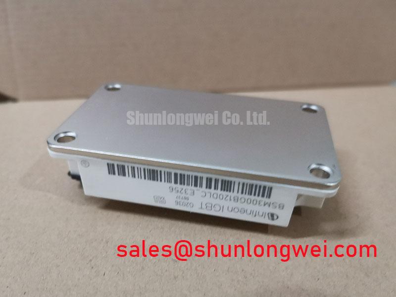
Clean the heat sink and module baseplate before applying thermal interface material. A uniform TIM layer is a general installation consideration; a thickness around 50 to 100 μm may be used as a bench starting range only when compatible with the selected material and mounting surfaces. The module manufacturer’s mechanical instructions remain controlling. Excess material can increase thermal resistance, while insufficient coverage can leave voids beneath the baseplate.
Check the heat sink for flatness, burrs, contamination, and local distortion before mounting. Baseplate convexity compensation should be handled through the approved mounting arrangement, not by forcing the module against an uneven surface. Start each screw by hand, bring the fasteners into contact progressively, and use a diagonal or manufacturer specified sequence so the baseplate settles evenly. The correct screw type, torque, tightening sequence, and retightening policy must be obtained from the mechanical documentation for this exact package.
After mounting, inspect the busbar and gate terminals for mechanical loading caused by misalignment. A busbar should not pull the module terminals sideways or place continuous stress on the case. Confirm electrical isolation after assembly, then perform low energy gate checks before applying the full DC link. Capture turn on, turn off, fault response, and regenerative waveforms at the module terminals. If overshoot, oscillation, or uneven temperature appears, review the complete commutation loop, gate return path, probe technique, cooling contact, and busbar symmetry before attributing the behavior to the module alone.