

Content last revised on September 21, 2026
Preventing Spurious Faults: High-di/dt Gate Firing: Pulse-Train Timing Guidelines for MCC255-14IO1
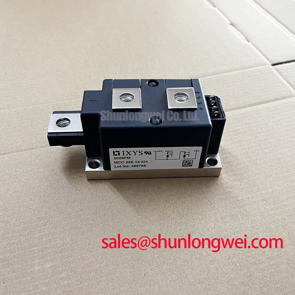
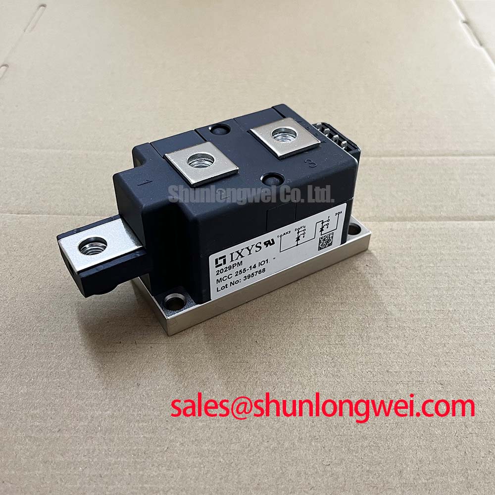
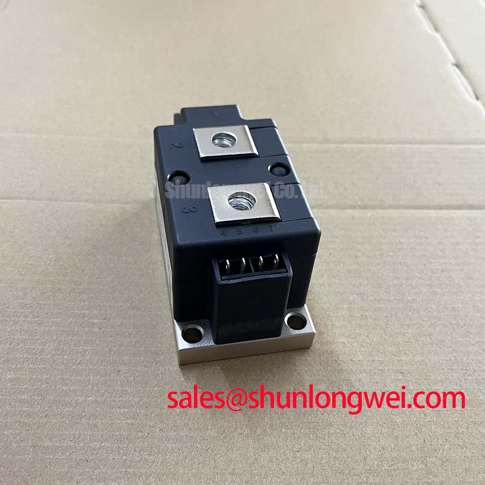
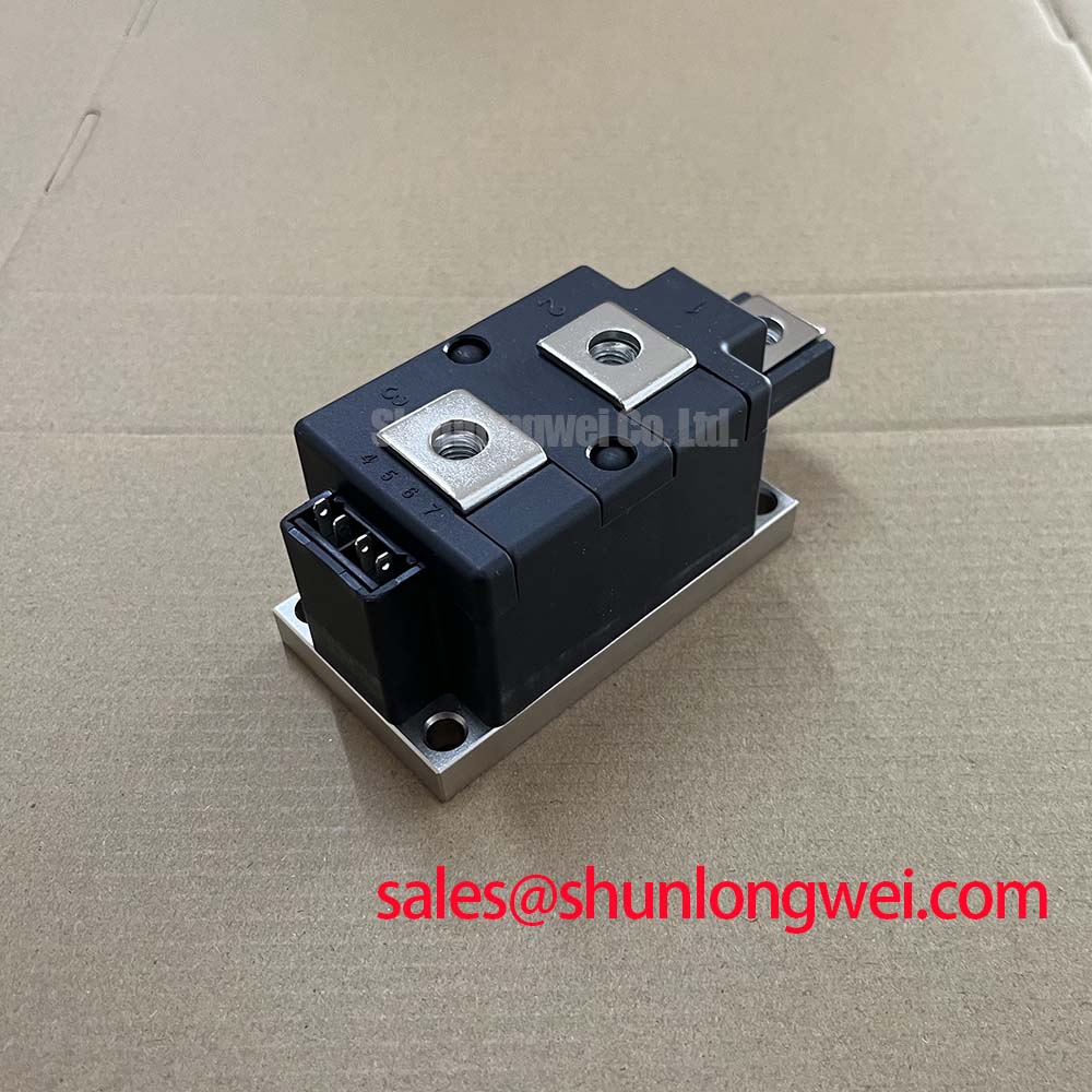
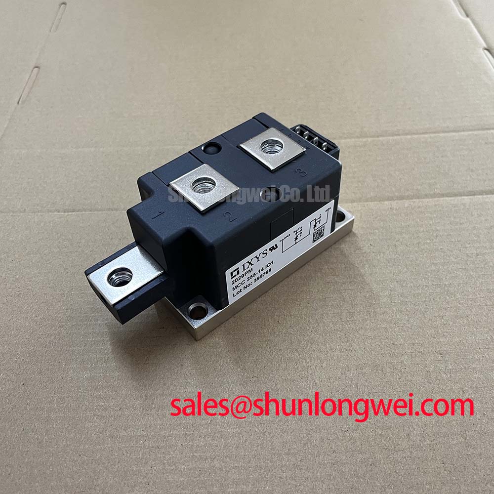
Start incoming inspection by recording the nameplate ratings, checking the module body for cracks or contamination, and comparing the terminal markings of the MCC255-14IO1 with the original equipment documentation before applying any test voltage.
The IXYS MCC255-14IO1 is a Dual Thyristor Module with an official rated voltage of 1400 V, an official rated current of 255 A, and a module-style housing. These are product-level ratings supplied for identification and engineering evaluation. They do not, by themselves, define the permissible current under every heatsink condition, switching waveform, ambient temperature, fuse arrangement, or phase-control duty.
| Manufacturer | IXYS |
| Part number | MCC255-14IO1 |
| Device category | Dual Thyristor Module |
| Rated voltage | 1400 V, Official Specification |
| Rated current | 255 A, Official Specification |
| Housing | Module, Official Specification |
During bench evaluation, identify the main power terminals and gate-related terminals from the applicable IXYS documentation rather than assuming that a visually similar module uses the same pin arrangement. With the device isolated and discharged, use resistance measurements to screen for an unexpected short between the main terminals. A diode-test reading can provide useful comparative information across matched paths, but a thyristor is not validated by one forward-voltage reading alone. The result depends on meter current, gate condition, stored charge, and the test connection.
A gate firing circuit for the MCC255-14IO1 should be assessed as a complete pulse path. The firing transformer or digital isolation stage, gate resistor, return conductor, connector, and local reference all contribute to the pulse seen at the terminal. A fast current edge can be useful for reliable triggering, but excessive loop inductance or an under-damped gate network can create ringing. The correct engineering method is to observe the gate-to-reference waveform at the module terminals with an appropriately rated differential measurement arrangement, then compare the measured pulse with the official gate-trigger, gate-current, and holding-current requirements for the exact device revision.
For phase-controlled SVC equipment, a single trigger pulse may be vulnerable to noise near the intended firing point. A pulse train can provide a practical control strategy, provided that the firing controller, isolation device, and gate dissipation limits are checked against the manufacturer’s data. Back-porch gate current should be evaluated as a controlled gate-drive parameter, not as an assumed fixed value or a substitute for the thyristor’s anode holding current. If the gate signal becomes intermittent, inspect the isolation supply, return path, connector pressure, and oscilloscope reference before attributing the problem to the power module.
The current path should remain physically separate from the sensitive gate loop. Minimize the area of the gate-drive loop, keep the gate return paired with its corresponding gate conductor, and avoid routing it alongside high-current commutation conductors. These are Design Considerations, not additional factory specifications for this part number. Any proposed gate-current rise-time target, multi-pulse interval, or back-porch level must be confirmed against the official datasheet and the isolation device’s common-mode transient capability.
Fuse coordination also requires the correct IXYS table for the application. The module’s 255 A rating must not be treated as a substitute for an I²t coordination check. The system designer should compare the prospective fault current, fuse clearing characteristic, repetitive overload profile, and the applicable thyristor I²t value from the manufacturer’s documentation. A replacement fuse with the same nominal current but a different clearing characteristic may change the semiconductor stress substantially.
Preventing Spurious Faults: Dynamic Voltage Sharing and RC Damping in Guidelines for MCC255-14IO1
In a high-voltage SVC or thyristor-switched capacitor branch, the wiring between the MCC255-14IO1, capacitor bank, reactor, fuse, and switching contact points forms part of the transient circuit. The first inspection should therefore follow the actual conductor path rather than relying on the schematic alone. Look for long unpaired conductors, loose busbar joints, damaged insulation, and measurement leads that introduce an unplanned capacitive or inductive coupling path.
RC snubber selection is application-specific. The resistor and capacitor must be selected from the switching waveform, repetitive voltage, pulse energy, capacitor dielectric limits, resistor pulse capability, and required damping behavior. No universal Rs or Cs value can be assigned to the MCC255-14IO1 from its 1400 V and 255 A ratings alone. This is an Engineering Recommendation: record the voltage across the device during switching, identify overshoot and ringing with a suitable probe, and verify the resulting peak against the system insulation and semiconductor operating limits.
A saturable reactor or other series impedance can alter the current rise seen by the thyristor. Its suitability depends on the source impedance, capacitor-bank configuration, firing sequence, prospective short-circuit current, and the physical placement of the damping components. Designers should verify both the initial current transient and the repetitive thermal condition. A circuit that appears acceptable during a low-energy bench test may behave differently when the full capacitor bank and grid impedance are connected.
Dynamic voltage sharing is also affected by tolerance, temperature, leakage, and switching history. Where multiple devices or branches operate in a coordinated arrangement, measure the voltage distribution under the real control sequence. Do not infer equal sharing from equal-looking wiring. The Power Semiconductor Selection Guide provides a broader engineering reference for comparing semiconductor stress, protection, and application constraints.
For a converter auxiliary supply associated with the control cabinet, the topology should be reviewed separately from the thyristor power path. A buck-boost family topology can produce different current and voltage stress from a direct regulated supply, while an interleaved boost arrangement can change input ripple behavior. These topologies are discussed in the Buck-Boost Converter Topology for High-Voltage Auxiliary Power Supplies and Interleaved Boost Converter for Reduced DC-Link Input Ripple Current references. They should not be used as evidence of an internal feature of this module.
Assembly Integrity & Layout Architecture: Implementing Surge Energy Dissipation and Clamping Voltage for MCC255-14IO1
Before fitting the module into a replacement assembly, clean the mounting surface, inspect the insulator arrangement, and confirm that the heatsink is flat and free of burrs. The correct mounting hardware, washer arrangement, thermal interface method, and tightening torque must come from the applicable mechanical documentation. A general mounting practice should not be presented as an MCC255-14IO1 factory parameter.
⚠️ Field Alert: Isolate and discharge the complete power assembly before disconnecting gate or auxiliary wiring, because control terminals can remain exposed to hazardous potential through external circuits.
For AC input protection, MOV selection should be based on the actual line-to-line and line-to-ground environment, continuous operating voltage, temporary overvoltage, surge class, energy capability, and coordination with upstream protection. IEC 61000-4-5 test conditions may help define a laboratory immunity assessment, but they do not automatically establish the field rating of a complete SVC installation or prove that the thyristor module independently meets an EMC requirement.
Place the clamping and damping network so that its connection inductance does not defeat its purpose. The design objective is to limit the voltage appearing at the semiconductor terminals during a surge or commutation event, while keeping leakage current, pulse energy, heat, and service clearances within the system limits. The selected MOV, RC network, fuse, and disconnect device must be evaluated as a coordinated protection network.
High-voltage terminal layout requires adequate creepage and clearance for the working voltage, pollution environment, insulation material, altitude, and applicable equipment standard. The 1400 V device rating is not a creepage or clearance specification. Engineers should verify the enclosure, barrier, busbar, and terminal geometry using the relevant insulation-coordination requirements for the finished equipment. High-altitude operation, humidity, contamination, and condensation require system-level assessment rather than a numerical assumption based only on the part number.
Where an industrial drive or SVC controller uses an optocoupler or digital isolator, review common-mode transient immunity against the measured switching edge and the isolation barrier layout. Keep the control reference, gate return, and power commutation path under deliberate control. A component’s isolation claim does not independently certify the complete control board, cabinet, or installation for EMC compliance.
MCC255-14IO1 Thermal-Electrical Optimization: Phase-Controlled Rectification, Firing Angle Practical Tuning
For phase-controlled rectification, firing-angle adjustment changes the average transferred power, line-current shape, displacement power factor, reactive demand, and device heating. The exact behavior depends on whether the load is resistive, inductive, capacitive, or part of a compensated network. A firing-angle range such as zero to 150 degrees should therefore be treated as a system test plan, not as an operating guarantee for the MCC255-14IO1.
Begin commissioning with a controlled low-energy condition and confirm the phase reference, gate sequence, and device voltage before increasing the applied power. Record the line voltage, load current, gate timing, device terminal voltage, heatsink temperature, and any commutation disturbance. If the measured waveform contains unexpected notches or a delayed current transfer, inspect the firing reference, isolation delay, reactor state, capacitor-bank condition, and wiring symmetry before changing the gate timing.
In a grid-tied static VAR compensator, a thyristor-switched capacitor branch may operate alongside reactors, filters, measurement transformers, and control protection. The SKKT91/08D can be reviewed as an example of a related power-semiconductor component in an associated rectification or power-conversion stage, but compatibility must be established from voltage class, current duty, terminal configuration, dynamic characteristics, and mechanical requirements rather than product category alone.
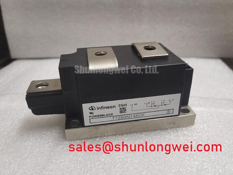
For a neutral comparison point during procurement, engineers may also review SKKT 106B14E. It should be treated as a separate reference device, not as an automatic substitute for the MCC255-14IO1. The original circuit documentation, protection coordination, gate-drive requirements, heatsink arrangement, and terminal geometry remain the controlling evidence for any replacement assessment.
Thermal verification should follow the actual duty cycle. Measure the case or heatsink temperature at the defined mounting location, inspect the thermal interface after the test, and correlate temperature rise with RMS current and firing pattern. If long motor cables or other transmission-line effects are present elsewhere in the installation, investigate reflected-wave voltage at the relevant load and switching nodes with suitable high-voltage measurement equipment; do not transfer a cable-related observation directly to the thyristor terminals without waveform evidence.
For incoming QA, keep a cold-state reference record for each accepted unit: visual condition, terminal identification, comparative resistance readings, diode-test observations where meaningful, and the insulation-test method used by the facility. The applied insulation test voltage and duration must be selected from the official device documentation and the safety procedure for the assembled equipment. No field failure rate, service-life figure, cosmic-ray FIT value, or single-event burnout limit should be inferred without an authoritative source and the relevant system conditions.