
Content last revised on September 10, 2026
Optimizing Heatsink Contact Pressure and Surface Roughness for Minimum Rth(c-s)
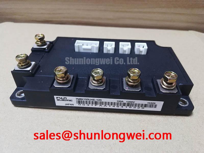
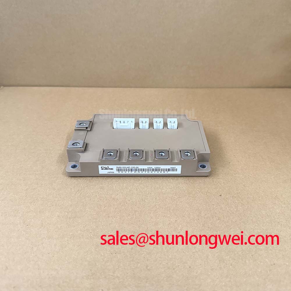
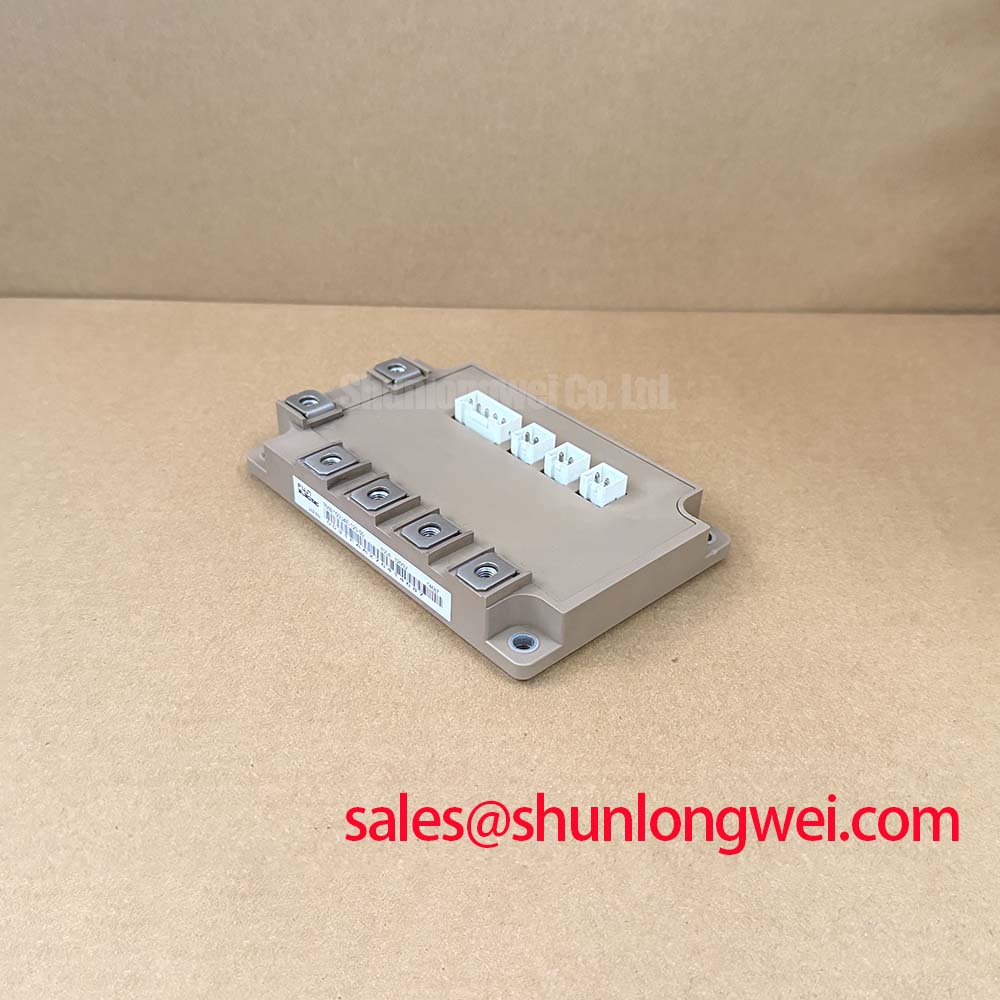
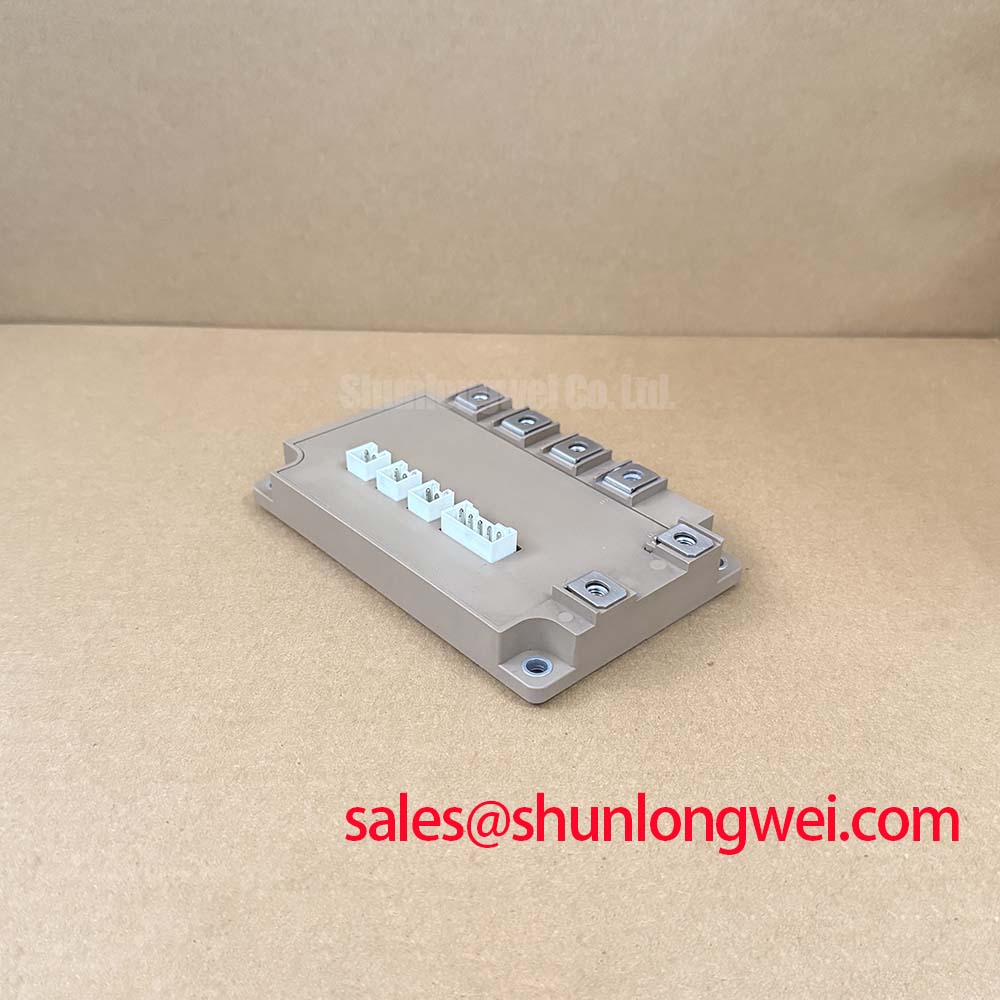
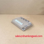
In high-capacity utility-scale 1500V solar string and central inverter systems, thermal management of power conversion stages dictates long-term operating reliability. The 7MBI100U4E-120-50 IGBT module from Fuji Electric integrates a complete 7-pack configuration (three-phase inverter plus dynamic braking stage) in a unified power package. The inverter section provides an official maximum power dissipation rating of PC = 540 W (Official Datasheet Specification) per switch at a continuous collector current rating of IC = 100 A at TC = 80°C (Official Datasheet Specification), with an absolute maximum operating junction temperature limit of Tj = +150°C (Official Datasheet Specification). Mitigating thermal bottlenecks between the copper baseplate and the system heatsink is vital to prevent localized silicon die over-temperature faults during peak irradiance cycles.
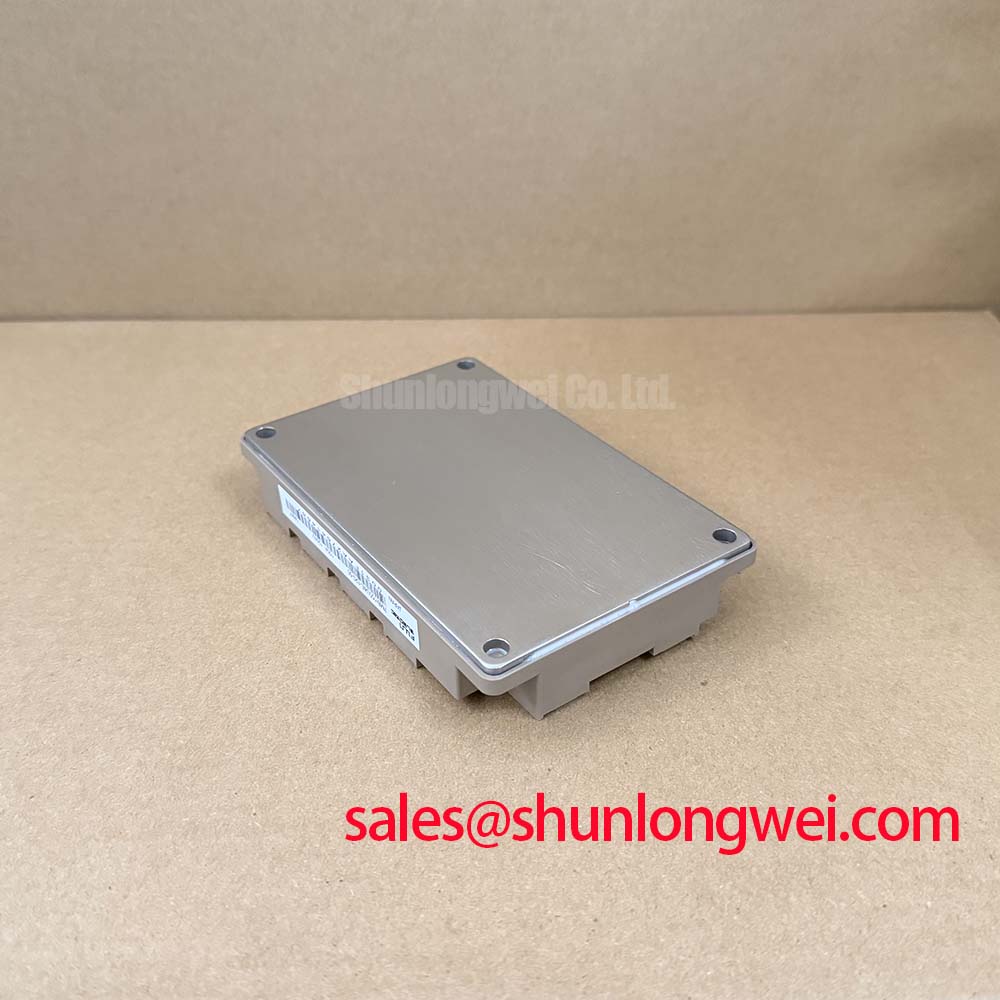
The total case-to-heatsink thermal resistance, Rth(c-s), depends directly on mechanical contact uniformity, thermal interface material (TIM) thickness, and mounting torque execution. When mating the module to a liquid-cooled cold plate or heavy aluminum extrusion heatsink, the mounting surface must meet strict mechanical tolerances: surface roughness should remain within Rz ≤ 10 μm, and surface flatness across the mounting footprint must not exceed 50 μm per 100 mm span (General Industry Design Consideration for Power Module Cold Plates).
Achieving a uniform, void-free thermal interface requires strict application control of thermal paste:
- TIM Thickness Control: Apply a homogeneous layer of high-performance thermal grease with a target thickness of 50 μm to 100 μm using a calibrated screen or steel stencil. Applying excess paste (>150 μm) increases thermal impedance and induces grease "pump-out" during repeated solar diurnal thermal cycles.
- Baseplate Pre-Bowing Compensation: The module baseplate features a slight engineered convex curvature to ensure that central die locations establish primary contact under clamping pressure. Applying uneven fastener torque can invert this curvature, creating an air void directly beneath high-loss inverter IGBT dies.
- Crosswise Torquing Sequence: Fasten the M5 mounting screws in a two-stage diagonal sequence. First, apply a finger-tight preliminary torque of 0.5 N·m across all positions to seat the baseplate evenly. Next, progressively torque all screws to the final operating specification of 2.5 N·m to 3.5 N·m (General Industry Design Consideration for M5 module baseplates).
⚠️ Field Alert: During field replacement inside inverter enclosures, technicians must inspect the heatsink for microscopic aluminum burrs around tapped screw holes. A single 0.2 mm metal burr prevents flush baseplate contact, elevating Rth(c-s) by up to 300% and triggering localized thermal runaway within minutes of operating at full rated load.
Active Miller Clamp Implementation & Parasitic Capacitive Turn-On Prevention
Operating inside 1500V solar string topologies exposes power semiconductor stages to steep voltage gradients, frequently exceeding dv/dt rates of 15 kV/μs during hard-switching transitions. With the 7MBI100U4E-120-50 rated at a maximum collector-emitter breakdown voltage of VCES = 1200 V (Official Datasheet Specification) and a gate-emitter voltage tolerance of VGES = ±20 V (Official Datasheet Specification), high dv/dt events across the complementary switch induce a displacement current through the internal collector-gate Miller capacitance (Cres / Cgc).
The displacement current injected into the gate node is defined by the physical relation:
IMiller = Cres × (dv/dt) (Engineering Calculation based on parasitic junction capacitance)
If this displacement current flows through the external turn-off gate resistance (Rg(ext)}) and the internal gate resistance, the resulting voltage drop at the gate terminal can exceed the IGBT threshold voltage (typically VGE(th)} = 5.5 V to 6.5 V), causing spurious turn-on and catastrophic DC-bus shoot-through. To suppress this parasitic turn-on mechanism without introducing excessive turn-off switching losses from an overly damped gate resistor, an active Miller clamp circuit should be integrated into the gate driver stage.
When the gate driver senses that VGE has fallen below 2.0 V during the turn-off sequence, an internal low-impedance MOSFET (RDS(on)} < 0.5 Ω) activates, pulling the gate node directly to the negative supply rail or ground. This diverts the Miller displacement current away from the primary gate path. Applying a true negative gate bias voltage between -5 V and -15 V (within the absolute maximum rating of VGES = ±20 V) provides dynamic noise margin against parasitic shoot-through transients.
Gate driver output stages must be sized to supply sufficient peak sourcing and sinking current:
Ig(peak)} = (VGE(on)} - VGE(off)}) / (Rg(ext)} + Rg(int)}) (Engineering Calculation based on total loop impedance)
Layout routing requires strict separation between the main high-current emitter power trace and the auxiliary Kelvin emitter terminal. The Kelvin emitter must return directly to the gate driver common reference plane, preventing inductive voltage drops (Ls} × di/dt) across the power lead from degrading gate turn-off stability. For diagnostic testing procedures and bench verification protocols on gate oscillation mitigation, consult the comprehensive Field Engineer’s Handbook. For advanced trench-gate topologies across generational platforms, review technical resources on Fuji Electric 7th-Gen X-Series IGBT Modules.
Isolated DC-DC Power Supply Sizing for High-Side Floating Gate Drivers
Utility-scale solar central inverters operate across wide DC-link voltage ranges, demanding galvanic isolation barriers on all high-side floating gate driver channels. To maintain signal integrity across transient grid-tie conditions, high-side DC-DC driver bias supplies must deliver continuous galvanic isolation exceeding 5 kV AC (RMS) with a Common-Mode Transient Immunity (CMTI) rating > 100 kV/μs.
Gate drive power supply capacity is dictated by the total gate charge (Qg), targeted PWM switching frequency (fsw), and baseline quiescent current consumption of the secondary driver circuitry. Sizing calculations follow the core dynamic power formula:
Pdriver = Qg × (VGE(on)} - VGE(off)}) × fsw + Pquiescent (Engineering Calculation based on gate charge dynamics)
At an inverter switching frequency of 15 kHz with gate bias voltages set to VGE(on)} = +15 V and VGE(off)} = -8 V (ΔVGE = 23 V), the driver power budget must account for module gate leakage current. The 7MBI100U4E-120-50 exhibits a maximum gate-emitter leakage current of IGES = ±500 nA at VGE = ±20 V (Official Datasheet Specification), representing negligible static loss relative to dynamic switching consumption.
Dead-time generation within the digital controller must account for high-temperature IGBT turn-off tail times. Under full junction temperature operation (Tj = +150°C), carrier recombination lifetimes increase, extending the turn-off fall time and storage delay. A dead-time window between 1.5 μs and 2.5 μs (Design Consideration for 1200V U4-series switching dynamics) ensures cross-conduction margins are preserved across ambient temperature swings.
For higher power sub-inverter stages requiring higher continuous current ratings beyond the 100 A envelope of this 7-pack configuration, the dual-pack 2MBI450XHA120-50 offers a continuous collector current rating of 450 A at VCES = 1200 V. For alternative topologies utilizing integrated freewheeling architectures, evaluate engineering specifications on Fuji Electric RC-IGBT Modules.
Transient Thermal Impedance (Zth(j-c)) & Multi-Layer Foster/Cauer Modeling
Solar string inverters experience abrupt load steps during rapid cloud transitions and low-voltage grid fault ride-through (FRT) events. During these short-duration overcurrent intervals, junction temperature swings cannot be predicted solely through steady-state thermal resistance Rth(j-c)}. Transient thermal impedance, Zth(j-c)}(t), must be evaluated using multi-layer thermal RC network models.
The inverter switches in the 7MBI100U4E-120-50 feature a typical collector-emitter saturation voltage of VCE(sat)} = 2.1 V (Official Datasheet Specification) and a maximum of VCE(sat)} = 2.7 V at IC = 100 A and VGE = 15 V (Official Datasheet Specification). The integrated dynamic braking IGBT switch is rated for IC = 50 A at TC = 80°C (Official Datasheet Specification) with a continuous pulsed peak rating of ICP = 100 A (Official Datasheet Specification) and a matching typical VCE(sat)} = 2.1 V at IC = 50 A (Official Datasheet Specification). Inverter switches support a peak pulsed rating of ICP = 200 A for a 1 ms pulse duration (Official Datasheet Specification).
Transient junction temperature rise under pulsed power dissipation P(t) is modeled mathematically as:
Tj(t) = Tc + P(t) × ∑ [ Ri × (1 - e-t / τi) ] (Engineering Calculation based on 4-element Foster thermal network)
The Foster network elements (Ri, τi) describe the physical layers of the power module stack: silicon die, direct bonded copper (DCB) ceramic substrate, solder interfaces, and the copper baseplate. During high-current transients, the thermal mass of the silicon chip dominates response times for pulses under 1 ms, while the DCB and baseplate absorb thermal energy over longer 10 ms to 500 ms windows.
Field Diagnostic & Electrical Measurement Protocol
Before replacing an inverter module, field service engineers must conduct a structured multimeter and insulation check to verify internal silicon integrity:
| Test Step | Measurement Nodes | Instrument Mode | Expected Reading / Pass Criteria |
|---|---|---|---|
| 1. Gate-Emitter Isolation | Gate (G) to Auxiliary Emitter (E) | Resistance (Ω) | > 10 MΩ (Open Circuit); < 100 Ω indicates gate oxide puncture |
| 2. Inverter Freewheeling Diodes | Emitter (Anode) to Collector (Cathode) | Diode Mode (V) | 0.35 V to 0.65 V forward drop; Open/Short indicates junction failure |
| 3. Collector-Emitter Blocking | Collector (C) to Emitter (E) | Diode Mode / Resistance | Open circuit in forward direction; > 1 MΩ DC resistance |
| 4. Brake IGBT & Diode Stage | Brake Collector to Emitter / Brake Diode | Diode Mode (V) | 0.35 V to 0.65 V diode drop; > 10 MΩ gate isolation |
| 5. Baseplate Isolation | All Terminals shorted to Module Baseplate | Megohmmeter (@ 1.0 kV DC) | > 100 MΩ; Isolation breakdown indicates substrate dielectric breach |