Content last revised on August 30, 2026
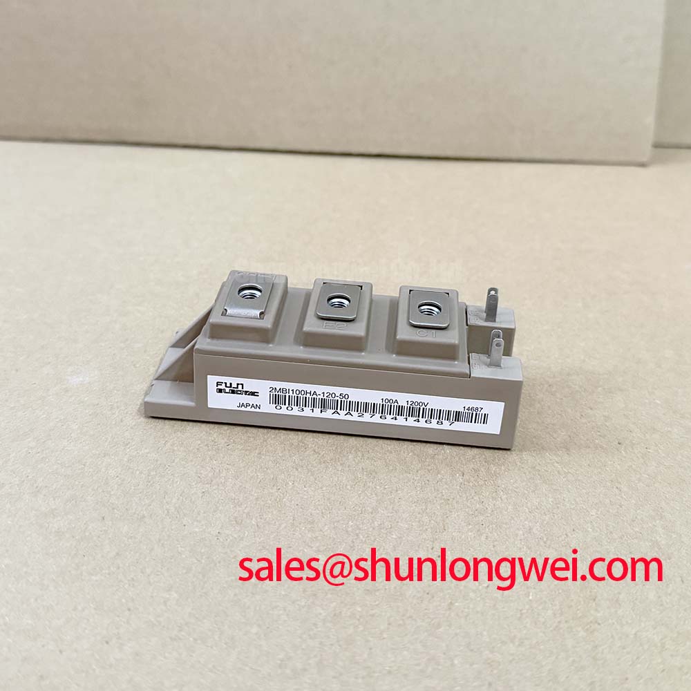
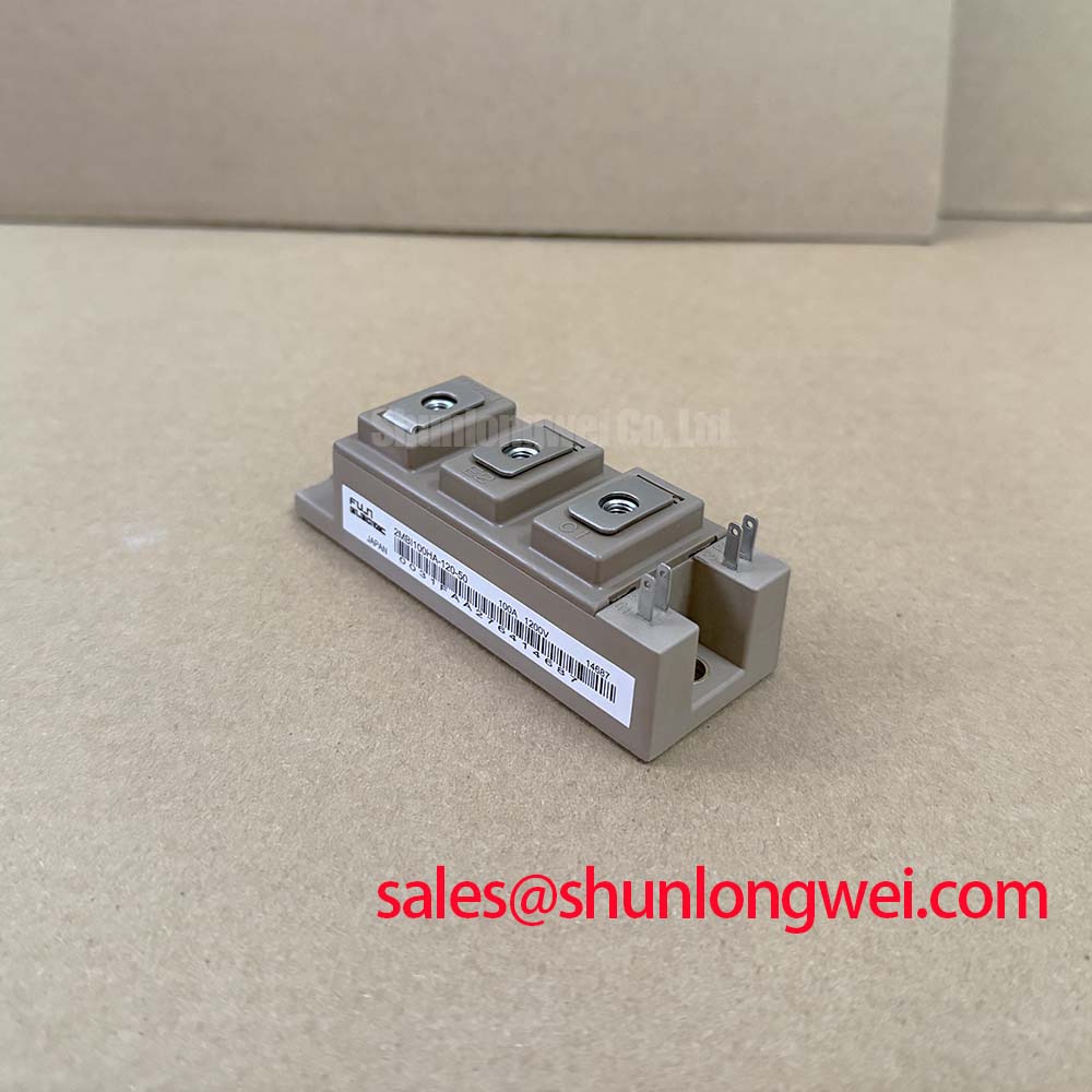
Incoming QA Verification & Electrical Ratings of the 2MBI100HA-120-50
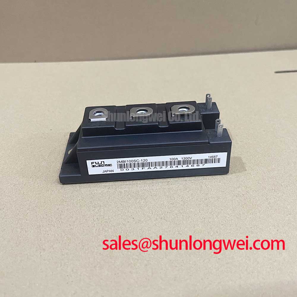
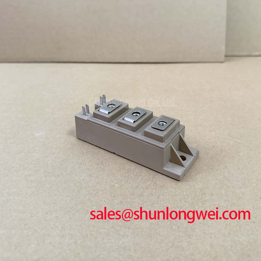
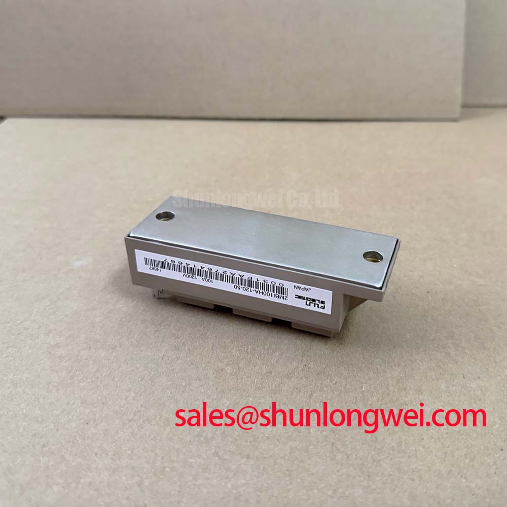
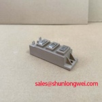
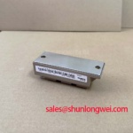
Incoming quality inspection of high-power dual-pack IGBTs requires rigorous static bench screening before modules enter inverter assembly or field replacement queues. The 2MBI100HA-120-50 dual IGBT module manufactured by Fuji Electric is engineered as a half-bridge switching stage primarily deployed in industrial motor drives and power conversion hardware. Verifying pin-to-pin integrity, gate oxide health, and internal freewheeling diode (FWD) health ensures baseline electrical conformance prior to mounting onto heatsink assemblies.
💡 Bench Tip: When unboxing the 2MBI100HA-120-50 on an ESD-safe workbench, always keep gate-emitter shorting pins or conductive foam in place until immediate test connection. Using a digital multimeter in diode-test mode at 25°C ambient, measure the forward voltage drop across the integrated FWD (terminals E1 to C1, and E2 to C2/E1). A typical healthy silicon junction registers between 1.15 V and 1.45 V. A reading approaching 0.00 V indicates an internal punch-through short, whereas an open-circuit reading signifies internal bond-wire lift-off.
| Parameter | Symbol | Value | Engineering Significance & Interpretation |
|---|---|---|---|
| Collector-Emitter Voltage | VCES | 1200 V | Rated at VCES = 1200 V (Official Datasheet Specification); provides voltage withstand margin for 380 V to 480 V AC nominal bus lines. |
| Continuous Collector Current | IC | 100 A | Rated at IC = 100 A at TC = 25°C (Official Datasheet Specification); defines continuous nominal conduction throughput. |
| Gate-Emitter Voltage | VGES | ±20 V | Absolute maximum gate-insulator stress rating (Official Datasheet Specification); driver rails must clamp within this window. |
| Collector Power Dissipation | PC | 1040 W | Maximum per-switch dissipation under idealized heatsink conditions at TC = 25°C (Official Datasheet Specification). |
| Isolation Voltage | Viso | 2500 V AC | 1-minute galvanic withstand barrier between baseplate and power terminals (Official Datasheet Specification). |
Desaturation (V_CE(sat)) Detection & Two-Stage Soft Turn-Off Short-Circuit Protection
In heavy-duty variable frequency AC motor drive applications, sudden phase-to-phase shorts or phase-to-ground faults expose the inverter bridge to catastrophic fault currents exceeding several times the nominal collector rating. The 2MBI100HA-120-50 relies on fast desaturation sensing to safeguard the silicon die within its Short-Circuit Safe Operating Area (SCSOA). The SCSOA defines an absolute maximum short-circuit duration of 10 µs under standard bus voltages before thermal runaway occurs.
When the IGBT exits saturation under high fault currents, the collector-emitter voltage rises abruptly while full gate bias remains applied. Gate driver ICs equipped with desaturation protection monitor this threshold through a high-voltage blocking diode. As highlighted in technical documentation for STMicroelectronics Galvanic Isolated Gate Drivers, desaturation sensing circuitry must incorporate a blanking time filter—typically configured between 1.5 µs and 3.0 µs (Typical Starting Point for bench tuning)—to bypass the initial turn-on voltage tail and prevent false tripping caused by capacitive displacement currents.
Once a fault condition is validated, standard hard shut-off must be strictly avoided. Abruptly interrupting a short-circuit current of 400 A to 600 A generates extreme inductive turn-off spikes across the internal parasitic loop inductance. Implementing a two-stage soft turn-off (2SSTO) lowers the gate voltage from +15 V down to an intermediate clamp level (such as +7 V to +9 V) for roughly 1.0 µs before pulling the gate to its negative rail. This controlled di/dt deceleration limits transient overvoltages safely below the 1200 V breakdown boundary without breaching SCSOA thermal limits.
Junction-to-Case Thermal Network Simulation under High-Pulsed Overloads
Heavy-duty AC motor drives frequently experience severe pulsed overloads during direct-on-line motor startup, locked-rotor conditions, or cyclic mechanical jamming. Evaluating the transient thermal impedance of the 2MBI100HA-120-50 ensures that peak junction temperature does not breach the critical 150°C operational limit. Transient heat transfer from the IGBT junction through the direct bonded copper (DBC) ceramic substrate to the copper baseplate is modeled using multi-element Foster and Cauer RC networks.
Under repeated high-current overload pulses, the thermal response depends on the transient thermal impedance Zth(j-c) rather than steady-state thermal resistance Rth(j-c). During a 10 ms overload surge, heat remains largely trapped within the silicon die and DBC ceramic layers before propagating into the main external heatsink. Maintaining adequate safety margins during high-torque bursts requires strict optimization of the physical interface between the module copper baseplate and the aluminum heatsink.
⚠️ Field Alert: Excessive or uneven thermal grease application can increase thermal resistance and accelerate module failure. Apply a uniform layer of high-performance thermal interface material (TIM) with a wet thickness of 80 µm to 100 µm (General Industry Design Consideration). Fasten the M5 mounting bolts incrementally using a cross-pattern torque sequence: pre-tighten to 1.0 N·m, followed by a final tightening torque of 2.5 N·m to 3.5 N·m (General Industry Design Consideration for M5 baseplate mounting). For detailed inspection protocols on mechanical flatness and junction thermal stress, refer to the Field Engineer’s Handbook.
To suppress transient voltage overshoots during high di/dt commutation, the DC bus layout must maintain a total parasitic loop inductance below 25 nH (Engineering Calculation based on a 100 A/µs turn-off slope). Placing low-inductance polypropylene film snubber capacitors directly across the module's positive and negative power terminals absorbs energy stored in the busbar inductance, clamping inductive spikes well below VCES = 1200 V.
Dynamic Gate Impedance Control for Robust Phase-Leg Dead-Time Operation
In a half-bridge topology, high dynamic dv/dt transitions on the switching node induce displacement currents through the Miller capacitance (Cres / Cgc) of the complementary inactive IGBT. If the gate-emitter impedance is insufficiently damped, this displacement current generates a voltage drop across the turn-off gate resistance that can exceed the gate threshold voltage VGE(th), leading to shoot-through across the DC bus.
To maintain robust operation during bridge dead-time transitions (typically set between 2.0 µs and 3.5 µs as a Design Consideration), gate drivers should implement negative off-state biasing between -5 V and -15 V, or utilize an active Miller clamp circuit. As documented in the Fuji Electric V-Series IGBT Application Manual, dynamic gate resistance should be decoupled using independent turn-on (RG(on)) and turn-off (RG(off)) paths via anti-parallel diodes. A lower RG(off) reduces dv/dt-induced gate bounce, while a calibrated RG(on) dampens free-wheeling diode reverse-recovery current snaps.
For systems requiring higher current handling capabilities or upgraded capacity, the related 2MBI400VB-060-50 provides an alternative switching configuration within the 600 V class for low-voltage, high-current drive architectures.
Suppression of 2x V_DC Voltage Doubling at Inverter-Driven Motor Terminals
Variable frequency drives driving AC induction motors over extended motor lead lengths (exceeding 20 to 50 meters) introduce severe transmission line impedance mismatches. The steep rise times (dv/dt exceeding 5 to 10 kV/µs) generated by the fast switching of the 2MBI100HA-120-50 propagate along the motor cable and encounter the high wave impedance of the motor stator windings. This impedance boundary causes full wave reflection, resulting in voltage doubling where peak terminal voltage approaches twice the nominal DC bus voltage (2x VDC).
On a 400 V / 480 V AC nominal mains system where the rectified DC bus operates around 560 V to 680 V DC, reflected wave peaks can exceed 1300 V at the motor terminals. This repetitive overvoltage stresses motor inter-turn winding insulation, generates localized partial discharge, and damages motor bearings via capacitive shaft currents.
Mitigating these transmission line reflection spikes involves inserting balanced dv/dt output chokes or LC sine-wave filters at the inverter output terminals. Sizing the series output choke to restrict inverter output dv/dt to below 500 V/µs (Design Consideration) smooths terminal voltage gradients, extends stator insulation lifespan, and prevents common-mode noise coupling back into sensitive logic circuits.