Content last revised on September 10, 2026
Benchtop Waveform Tuning for Four Quadrant Power Flow with 6MBI75S-120-02
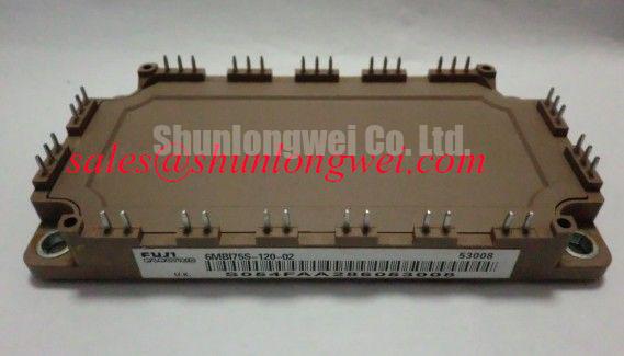
Begin incoming inspection with the module fully isolated: check the package for cracks, contamination, loose terminals, or deformation, then compare the marked terminal arrangement with the original inverter wiring record before applying any test voltage. The supplied product data identifies the Fuji Electric 6MBI75S-120-02 as an IGBT Module with a listed current rating of 75.0 A and a listed voltage parameter of 20.0 V. These values are treated here as official specification data supplied for this product listing; engineers should confirm the exact parameter designation, test conditions, and complete electrical limits against the applicable Fuji Electric documentation before commissioning.
For a commercial string inverter or micro grid energy storage converter, the module may be evaluated within a four quadrant power flow arrangement in which the battery rack and inverter DC link exchange energy in both directions. The practical bench objective is to observe switching voltage, collector current, gate signal timing, and thermal response during charge, discharge, regeneration, and power factor control. The module itself does not define the complete operating envelope of the converter. The DC link, gate driver, busbar arrangement, protection system, cooling assembly, and control firmware determine whether the application is suitable.
During a cold state check, use a properly rated digital multimeter in diode mode only after confirming that the DC link capacitors are discharged and the gate terminals are controlled against accidental static charging. Check the expected semiconductor junction paths according to the original circuit documentation, recording the polarity and the reading direction rather than treating one unverified meter value as a pass or fail threshold. An unexpected open circuit, unstable reading, or low impedance in both directions may justify comparison with a known good module and an oscilloscope based gate and power path inspection.
Four quadrant operation can produce repeated heating and cooling cycles during peak shaving, especially when the battery system changes rapidly between importing and exporting power. This is a Design Consideration rather than a confirmed lifetime characteristic of this specific part. Designers should examine junction temperature variation, case temperature distribution, switching frequency, overload duration, and cooling response together. A thermal camera can help locate uneven mounting or busbar heating, while thermocouples placed at defined case reference points provide a more repeatable comparison between test runs.
Keep the commutation path compact and symmetrical so that stray inductance does not create avoidable turn off overshoot. The required electrical clearance and creepage are system determined by working voltage, insulation category, pollution environment, altitude, and enclosure construction. During waveform tuning, verify the measured peak voltage against the applicable module blocking limit and the DC link transient envelope. Do not infer clearance requirements from the package name alone.
When a replacement is being assessed for a service repair, compare the original topology, current duty, gate drive arrangement, terminal orientation, mechanical footprint, and cooling interface. A related device such as 6MBI300U-120 should be treated as a separate evaluation item, not an automatic substitute. The system engineer must verify electrical ratings, switching behavior, protection coordination, and mechanical compatibility before any interchange decision.
Benchtop Waveform Tuning for Hard Switching Transients on 6MBI75S-120-02
Hard switching transients should be investigated by probing the gate to emitter voltage and collector to emitter voltage with suitable isolated measurement equipment while monitoring current at the commutation loop. A ringing waveform can involve gate loop inductance, common emitter impedance, probe placement, driver output impedance, DC link layout, or an interaction between the module and its freewheel path. The correct response is to compare the complete signal path with the intended schematic and a known good switching waveform.
Short circuit protection requires coordination between detection, gate driver action, semiconductor behavior, and the upstream fuse or electronic protection stage. The supplied application brief refers to Type I and Type II short circuit detection within less than 10 µs and to short circuit safe operating area evaluation. Those values are application targets stated for the requested design discussion, not confirmed manufacturer limits for this listing. The applicable Fuji Electric data must be checked for short circuit withstand time, test conditions, gate voltage, junction temperature, and repetition restrictions before the protection sequence is approved.
A two stage soft turn off strategy is commonly evaluated when an overcurrent or desaturation event is detected. The driver may first reduce gate current in a controlled manner and then complete turn off with a stronger clamp, but the timing, voltage level, and current profile must be established by the system designer through double pulse and short circuit testing. The purpose is to limit the rate of current collapse and the associated inductive voltage rise without allowing the fault current to persist beyond the device protection envelope.
Gate drive sourcing and sinking capability should be selected from the required gate charge, switching speed, driver output impedance, isolation behavior, and allowable gate voltage excursion. An external gate resistance is a Typical Starting Point for bench tuning, not a fixed value for this module. Increase or decrease the damping resistance while observing turn on loss, turn off loss, gate ringing, collector voltage overshoot, and driver heating. Any final value must be validated at the highest intended bus voltage, current, temperature, and wiring parasitic condition.
Desaturation protection should be checked with the actual fault blanking behavior and soft turn off path installed. A false trip may involve sensing layout, diode recovery, driver common mode movement, or a poorly controlled reference connection. A missing trip cannot be attributed to the IGBT alone without checking the desaturation supply, sense lead routing, gate clamp, isolation barrier, and fault latch. Use a current limited test arrangement and confirm that the protection circuit returns to a defined state after the fault is removed.
Fuji Electric provides application information for Fuji Electric Brake Chopper IGBT Modules. That material can support general understanding of chopper related power switching, but it should not be read as a substitute for the exact 6MBI75S-120-02 datasheet or as evidence that this module independently satisfies an entire inverter protection or EMC design.
Isolated DC-DC Power Supply Sizing for High Immunity Gate Drive Integration
Inspect the isolated gate supply before connecting the module by measuring output stability under the driver load, checking polarity at the gate driver connector, and confirming that the isolation barrier is not bypassed through oscilloscope grounds, auxiliary shields, or communication cables. The system integrator should verify the required supply voltage from the original driver documentation. The supplied product data does not specify a gate supply voltage, isolation rating, or common mode transient immunity value for this IGBT module.
Reinforced galvanic isolation and high common mode transient immunity are Design Considerations for an inverter gate drive, particularly when the switching node moves quickly relative to the control ground. The requested design brief cites a barrier requirement above 5 kV and a CMTI target above 100 kV/µs. These are system design targets, not official ratings established for the 6MBI75S-120-02 by the product data supplied here. Select the isolated DC DC converter, digital isolator, optocoupler, transformer, and insulation system from their own certified specifications and verify the assembled barrier under the intended operating conditions.
Spurious gate pulses are often investigated by monitoring the isolated supply output, input logic waveform, gate to emitter waveform, and switching node at the same time. If the gate signal changes during a high voltage transition, check the isolator CMTI data, driver reference routing, Miller clamp behavior, common mode displacement current, and local decoupling. The diagnosis should remain measurement based because a similar symptom can arise from inadequate supply impedance, incorrect probing, connector coupling, or control board timing.
Gate supply capacitors must support the driver’s high frequency charging and discharging current without excessive local voltage movement. Their value, dielectric type, voltage rating, placement, and ripple capability are determined by the driver current profile and switching frequency. If a bootstrap supply is used elsewhere in the gate circuit, verify the capacitor charging path, diode recovery behavior, duty cycle restrictions, and available refresh interval from the original driver design. Do not assume that a bootstrap arrangement is compatible with every four quadrant operating state.
Route isolated control signals away from high di/dt power loops and avoid unnecessary parallel runs with collector or emitter conductors. The required board clearance and creepage must be calculated from the system insulation requirements rather than copied from a generic module outline. During fault testing, confirm that the gate driver remains in its defined off state, that the fault latch operates as intended, and that reset behavior does not create a second uncontrolled pulse.
💡 Bench Tip: Use ESD protection and record a cold state baseline for gate to emitter impedance and diode path behavior before comparing a returned module with a known good unit.
Assembly Integrity and Thermal Capacitance Evaluation for Pulsed Operation
Thermal evaluation should start with a clean mounting surface, an even interface layer, and a repeatable fastener sequence, followed by measurement of case temperature at the same physical reference point for every test. The package is specified as Module; the supplied data does not provide a case drawing, thermal resistance value, transient thermal impedance curve, maximum junction temperature, or mounting torque. Those values must be obtained from the relevant Fuji Electric documentation rather than inferred from the 75.0 A listing.
Under pulsed overload, junction temperature does not follow case temperature instantaneously. A transient thermal model represents the semiconductor path through several thermal resistance and capacitance sections, allowing the engineer to estimate how a short power pulse affects junction temperature before heat reaches the heatsink. This is an Engineering Calculation only when the model coefficients come from an authoritative thermal impedance curve or a validated laboratory measurement. Without those inputs, the calculation can show trends but cannot establish a safe peak junction temperature.
For battery charge and discharge cycling, record pulse duration, repetition interval, electrical loss, case temperature, heatsink temperature, coolant or airflow condition, and ambient temperature. Compare the measured thermal waveform during positive and negative power flow because current paths and switching losses may not be identical. A rising case temperature with a stable electrical waveform may point toward interface or cooling behavior, while abnormal electrical overshoot can increase loss before a visible thermal change occurs. These observations are diagnostic clues, not single cause conclusions.
Check the mechanical interface for rocking, uneven contact, contamination, and excessive interface material. Use the fastener specification and mounting procedure associated with the exact package drawing. If the original assembly uses an insulating sheet, thermal pad, or liquid compound, verify its thickness, dielectric capability, aging behavior, and compatibility with the heatsink. The module’s electrical isolation must be verified as an assembled system, including the baseplate, thermal interface, heatsink, and mounting hardware.
Thermal capacitance is also relevant to short peak shaving events. A large heatsink may keep the case temperature relatively stable while the junction experiences rapid internal heating, whereas repeated pulses can gradually move the entire assembly toward a higher temperature. Engineers should calculate peak temperature margins from validated transient thermal data and then confirm them with instrumented switching tests. If the thermal model and measured case waveform disagree, inspect loss estimation, sensor placement, interface uniformity, and switching waveform distortion before changing the cooling design.
For broader engineering background on heat spreading, insulated metal substrate approaches, and double sided cooling concepts, consult The Advanced Thermal Management Revolution. The guide provides system level context; it does not establish construction details or thermal performance values for this Fuji Electric module.
Before energizing a repaired commercial string inverter or micro grid storage converter, complete an insulation resistance and dielectric withstand review using the equipment manufacturer’s approved test procedure, then verify gate polarity, interlock operation, fuse coordination, current sensing, and cooling response at reduced test energy. The 6MBI75S-120-02 listing identifies a 20.0 V voltage parameter and 75.0 A current parameter, but the complete application boundary remains dependent on the original technical documentation and the assembled converter design.