Shunlongwei Co. ltd.
IGBT Module / LCD Display Distributor
Customer Service
+86-755-8273 2562
IGBT Module / LCD Display Distributor
The structure of an IGBT transistor is much more complex than that of a MOSFET or bipolar junction transistor (BJT). It combines the characteristics of both devices and has three terminals: a gate, a collector, and an emitter. The device behaves like a MOSFET in terms of gate drive. Its current-carrying path is very similar to the collector-emitter path of a BJT. Figure 1 shows the equivalent device circuit of an n-type IGBT.
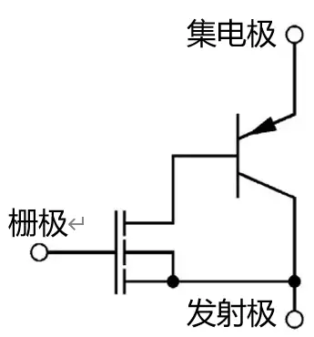
Figure 1. Equivalent circuit of IGBT
1. Understand the basic driver
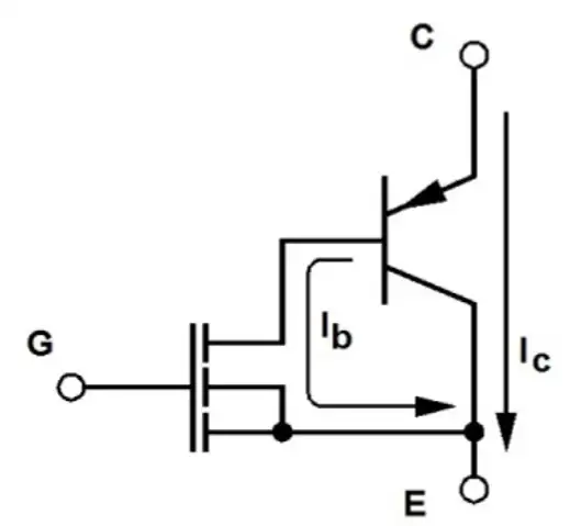
Figure 2. IGBT on-current
To turn a BJT on and off quickly, the gate current must be hard driven in each direction to move carriers into and out of the base region. When the MOSFET’s gate is driven high, there is a low-impedance path from the bipolar transistor’s base to its emitter. This causes the transistor to turn on quickly. Therefore, the higher the gate level is driven, the faster the collector current will start flowing. The base and collector currents are shown in Figure 2.
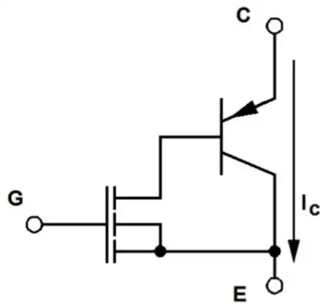
Figure 3. IGBT turn-off current
The shutdown scenario is a little different, as shown in Figure 3. When the gate level of the MOSFET is pulled low, there will be no current path for the base current in the BJT. The absence of base current will induce a shutdown process; however, for fast shutdown, current should be forced into the base terminal. BJTs turn off relatively slowly since there is no mechanism available to sweep carriers away from the base. This results in a phenomenon known as tail current, since the charge stored in the base region must be swept away by the emitter current.
It is obvious that a faster gate drive dv/dt rate (due to higher gate current capability) will turn the IGBT on and off faster, but for the switching speed of the device (especially the turn-off speed) There are inherent limitations. It is because of these limitations that switching frequencies are usually in the range of 20kHz to 50kHz, although in special cases they can also be used in faster and slower circuits. IGBTs are commonly used in high power (Po > 1 kW) circuits in resonant and hard switching topologies. Resonant topologies minimize switching losses because they are either zero-voltage or zero-current switching.
Slower dv/dt rates improve EMI performance (when it comes to this aspect) and reduce spike formation during turn-on and turn-off transitions. This comes at the expense of reduced efficiency because the turn-on and turn-off times are longer.
Two secondary conduction
MOSFETs suffer from a phenomenon called secondary conduction. This is due to the very fast dv/dt rate of the drain voltage, which can range from 1000–10000 V/us. Although IGBTs generally do not switch as fast as MOSFETs, they can still experience very high dv/dt levels due to the high voltages used. If the gate resistance is too high, it will cause secondary conduction.
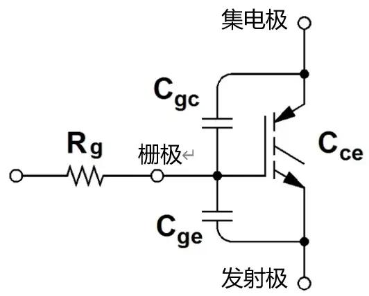
Figure 4. IGBT with parasitic capacitance
In this case, when the driver pulls the gate level low, the device starts to shut down, but the increased voltage on the collector creates a voltage on the gate due to the Cgc and Cge voltage divider. If the gate resistance is too high, the gate voltage can rise enough to cause the device to turn back on. This results in high power pulses that can cause overheating and in some cases even damage the device.
The limiting formula for this problem is:
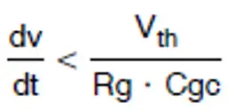
in,
dv/dt is the rate at which the voltage waveform on the collector rises during turn-off.

Rg is the total gate resistance
Cgc is the gate-emitter capacitance
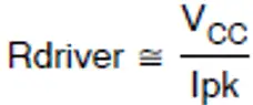
It should be noted that Ciss on the datasheet is the parallel equivalent of the Cge and Cgc capacitors. Similarly, Rg is the series sum of the gate driver impedance, physical gate resistance, and internal gate resistance. The internal gate resistance can sometimes be calculated from the data sheet. If it cannot be calculated, it can be measured by using an LCR bridge and shorting the collector-emitter pins, then measuring the equivalent series RC at a frequency close to the switching frequency. If you are using a FET output stage, you can find the driver impedance in its datasheet. If it cannot be found on the datasheet, an approximate calculation can be made by taking the peak drive current to its rated VCC level.
(Formula 2)
Therefore, the maximum total gate resistance is:
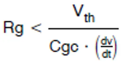
(Formula 3)
The maximum dv/dt is based on the gate drive current and the circuit impedance around the IGBT. If high value resistors are used for gate drive, this needs to be verified in an actual circuit. Figure 5 shows the turn-off waveforms of three different IGBTs in the same motor control circuit. In this application, dv/dt is 3500 V/s.
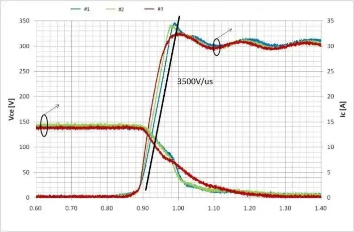
Figure 5. Turn-off waveforms of three IGBTs
For this case, IGBT #2 has a typical Cgc of 84 pF and a threshold gate voltage of 7.5 V (at 15 A).
Using the above formula, the maximum total gate resistance of this circuit is:
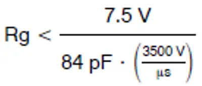
(Formula 4)
Rg < 25.5Ω.
Therefore, if the internal gate resistance is 2Ω and the driver impedance is 5Ω, the absolute maximum gate resistance used should be 18Ω. In practice, a smaller maximum value (e.g. 12Ω) is recommended due to variations in IGBT, driver, board impedance and temperature.
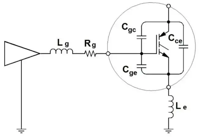
Figure 6. Equivalent gate drive circuit
Three gate ringing
Eliminating the external gate resistor may result in the best high frequency performance while ensuring that secondary turn-on does not occur. In some cases this may work, but it may also cause oscillation due to impedance in the gate drive circuit.
The gate drive circuit is a series RLC resonant circuit. The capacitance is mainly due to IGBT parasitic capacitance. The two inductors shown are derived from a combination of the board trace inductance and bonding wire inductance of the IGBT and driver.
With little or no gate resistance, the resonant circuit will oscillate and cause high losses in the IGBT. At this time, a large enough gate resistance is needed to suppress the resonant circuit and thereby eliminate oscillation.
Since inductance is difficult to measure, it is also difficult to calculate the appropriate resistor. The best way to minimize the minimum gate resistance required is to use a good layout procedure.
The path between the driver and the IGBT gate should be as short as possible. This applies to the entire circuit path of the gate drive as well as the ground return path. If the controller does not include an integrated driver, it is more important to place the IGBT driver close to the gate of the IGBT than to place the input of the gate driver to the PWM output of the controller. The current from the controller to the driver is very small, so the effect of any stray capacitance is much smaller than the effect of high current and high di/dt levels from the driver to the IGBT. Short, wide traces are the best way to minimize inductance.
Typical minimum driver resistance range is 2Ω to 5Ω. This includes the driver impedance, external resistor value and internal IGBT gate resistance value. Once the board layout is designed, the gate resistor values can be determined and optimized.
4. Summary
This article gives guidelines for maximum and minimum gate resistor values. There is a range of values between these limits by which the circuit can be tuned for maximum efficiency, minimum EMI, or other important parameters. Picking a safe value between these extreme values in your circuit design ensures that the design is robust.