
Shunlongwei Co. ltd.
IGBT Module / LCD Display Distributor
Customer Service
+86-755-8273 2562
IGBT Module / LCD Display Distributor
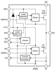
Called LMG2610, the IC includes a pair of GaN transistors in a half-bridge, gate drivers, a bootstrap diode and a high-side gate-drive level shifter, all in a 9 x 7mm QFN package.
The power transistors are asymmetric (170mΩ low side and 248mΩ high side) to optimise them for active-clamp use.
A “typical application shows the LMG2610 pairing with the UCC28782 controller to create a 65W USB-PD charger”, said TI.
For EMI and ringing control, both high and low-side drives have an independently programmable (by resistors) choice of turn-on slew rates (low-side = 20, 50, 70 or 140V/ns. High-side = 20, 65, 90 or 165V/ns).
On the low-side, there is current-sense emulation which “reduces power dissipation compared to the traditional current-sense resistor and allows the low-side thermal pad to be connected to the cooling PCB power ground”, said TI.
To reduce voltage drop, the bootstrap ‘diode’ is actually a third GaN transistor, switched by a control circuit. It “allows more complete charging of the BST-to-SW [see diagram] capacitor since the on-state GaN bootstrap transistor does not have the forward voltage drop of a traditional bootstrap diode”, according to the company. “The switched GaN bootstrap transistor also avoids the traditional bootstrap diode problem of BST-to-SW capacitor over-charging due to off-state third-quadrant current flow in the low-side half-bridge GaN power transistor.”
Protection features include an output transistor turn-on interlock, under-voltage lock-out, cycle-by-cycle current limit and over-temperature shut-down.
The IC needs a 10 – 26V supply (via AUX pad). It consumes 3.1mA operating, and a maximum of 80µA when the enable pad is not asserted.
View more : IGBT modules | LCD displays | electronic components
