Shunlongwei Co. ltd.
IGBT Module / LCD Display Distributor
Customer Service
+86-755-8273 2562
IGBT Module / LCD Display Distributor
“With the continuous improvement of the communication rate of Electronic systems, the problem of signal integrity in the interconnection area between BGA packages and PCBs has become more and more prominent. Design and optimize the high-speed BGA package and PCB differential interconnect structure, focusing on the analysis of the differential wiring method, signal layout method, signal hole/ground hole ratio, wiring layer and via stubs in the package and PCB interconnect area. Specific effects of high-speed differential signaling performance and crosstalk.The full-wave electromagnetic field simulation software CST is used to establish a 3D simulation model. Finally, the time-frequency domain simulation verifies that the optimization method can effectively improve the transmission performance of high-speed differential signals, reduce crosstalk between signals, and achieve better signals.
“
Abstract: With the continuous improvement of the communication rate of electronic systems, the signal integrity problem of the BGA package and the PCB interconnection area is becoming more and more prominent. Design and optimize the high-speed BGA package and PCB differential interconnect structure, focusing on the analysis of the differential wiring method, signal layout method, signal hole/ground hole ratio, wiring layer and via stubs in the package and PCB interconnect area. Specific effects of high-speed differential signaling performance and crosstalk. The full-wave electromagnetic field simulation software CST is used to establish a 3D simulation model. Finally, the time-frequency domain simulation verifies that the optimization method can effectively improve the transmission performance of high-speed differential signals, reduce crosstalk between signals, and achieve better signal isolation.
In recent years, Ball Grid Array (BGA) packages have become a widely used package type for high-speed ICs due to their small size, many pins, and good signal integrity and heat dissipation. In order to adapt to high-speed signal transmission, the chip mostly adopts the differential signal transmission method. As the number of chip I/O pins increases, the pitch of BGA solder joints is getting smaller and smaller, and the parasitic effects generated by the differential interconnect structure composed of solder joints, vias and printed lines will lead to attenuation, crosstalk, etc. A host of signal integrity issues pose serious challenges to high-speed interconnect designs. At present, scholars at home and abroad still focus on the modeling and simulation of horizontal transmission lines or single vias in the research of board-level signal integrity, and the frequency is mostly within 20 GHz. The transmission performance and coupling problems of differential interconnect structures including vias and transmission lines are rarely studied. There are few techniques to reduce crosstalk between vertical vias in the package and PCB interconnect areas.
This paper designs and optimizes the high-speed BGA package and the PCB differential interconnect structure. It focuses on analyzing the specific effects of improving the differential wiring method, signal layout method, signal hole/ground hole ratio, wiring layer and back drilling on improving high-speed differential signal transmission performance and crosstalk. The 3D simulation model is established by using the full-wave electromagnetic field simulation software CST Microwave Studio. The simulation frequency up to 40 GHz validates the effectiveness of the optimization method in both time and frequency domains.

1 Physical model
1.1 Differential interconnect structure
In high-speed signal transmission, differential signaling is widely used due to its advantages of reducing track collapse and electromagnetic interference, increasing gain, and eliminating common-mode noise and switching noise. The high-speed differential signal propagates through the IC package to each layer of the PCB. In order to realize the electrical connection between the BGA package substrate and each layer of the PCB, a differential interconnection structure is formed by horizontal differential lines and vertical differential vias, as shown in Figure 1.

Figure 1 Vertical interconnection structure between BGA package and PCB board
1.2 Simulation environment and parameter settings
The simulation environment used in this paper is the full-wave electromagnetic field simulation software CST Microwave Studio, which integrates time-frequency domain algorithms and includes multiple full-wave and high-frequency algorithms. It can simulate S parameters under any structure and material, and can be combined with circuit design. Software co-simulation. Several optimization schemes are established by the CST microwave studio to establish a three-dimensional physical model. The laminated structure of the PCB is shown in Figure 2. The PCB board has a total of 12 layers. layer), the 2nd, 4th, 6th, 7th, 9th and 11th layers are power or ground layers. The board thickness is 97.6 mil, the board dielectric constant is 3.8, and the loss tangent is 0.012. The 0.8 mm pitch BGA fan-out via pitch is 31.4 mil, the via diameter is 8 mil, the line width/line spacing is 5 mil, and the differential trace is on the 10th layer. .
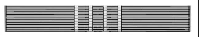
Figure 2 Cross-sectional view of the laminated structure of the PCB board
2 Optimization and Design
This section focuses on design optimization from four aspects to improve the transmission performance of high-speed differential signals and the crosstalk between signals. They are differential wiring method, signal distribution method, signal hole/ground hole ratio, wiring layer selection and via stub. The results of the CST simulations, presented in the form of S-parameters, at simulation frequencies up to 40 GHz, verify the effectiveness of the described optimization method in both the time and frequency domains.
2.1 Wiring method
When the differential signal is drawn out from the via, different wiring methods will have a great impact on the transmission characteristics of the differential signal. If the transmission lines cannot be of equal length and distance, the signal will be distorted and common mode noise will be generated. As shown in Figure 3, when the signal is drawn from the via hole, three wiring methods are adopted, 0°, 90° corner, and 45° corner, and there are two isolated ground holes around each pair of differential vias. The wiring is on the 10th layer of the PCB board.
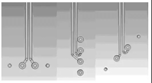
Figure 3 Three differential line lead-out methods
Figure 4 shows the insertion loss of the above three different wiring methods. Obviously, the first horizontally symmetrical way has the best transmission performance. The most important thing for differential signals is equal length and equal distance. The purpose of equal length is to ensure the accuracy and symmetry of the timing. Any delay difference or misalignment between the two transmission lines will cause the differential signal to be distorted and make some differential signals become. Common mode signal, which produces electromagnetic interference. The purpose of the equidistant is to maintain the consistency of the differential impedance. The 45° and 90° corners cannot be absolutely equidistant during wiring, resulting in phase difference and common mode noise.

Figure 4 Insertion loss of differential pair under different wiring methods
Figure 5 and Figure 6 show the common-mode noise generated by the three wiring methods from the frequency and time domains, respectively. Both 45° and 90° corners generate much higher common-mode noise than 0°, and 45° corner routing is slightly better than 90° corner routing.

Figure 5 Comparison of common mode noise frequency domain under different wiring methods

Figure 6 Time domain comparison of common mode noise under different wiring methods
As a rule of thumb, in order to maintain the dislocation within 10% of the rising edge of the signal, the lengths of the two lines are required to be matched to within 10% of the space extension of the rising edge. In this case, the matching requirements for the total trace length are as follows:
ΔL =0.1×RT×v
In the formula: ΔL represents the maximum length deviation between the two traces when the dislocation is maintained within 10% of the rising edge; RT represents the rising edge of the signal; v represents the propagation speed of the differential signal. If the propagation speed of the signal is roughly 6 in/ns and the rising edge is 100 ps, the lengths of the two traces should be matched so that their deviation is less than 60 mils. As the rise time of high-speed signals is getting shorter and shorter, the dislocation budget left to due to the deviation of trace length is becoming smaller and smaller, making the matching between trace lengths more and more important.
Therefore, in practical applications, the horizontal symmetry of 0° should be used as far as possible to achieve the purpose of equal length and equal distance.
2.2 Signal Distribution Mode
The pins of the BGA package are connected to other layers of the PCB board through vias during fan-out. Dozens of pairs of differential pairs are simultaneously high-density and long-line parallel. Signals transmitted on differential lines will cause crosstalk to adjacent transmission lines[9]. Since the arrangement of BGA solder joints is fixed, the positions of pads and vias depend on the distribution of solder joints, and a reasonable BGA pin signal layout can improve the crosstalk between differential pairs. See Figure 7 for different signal distribution modes.
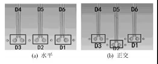
Figure 7 Different signal distribution methods
As shown in Figure 7, there are two layout modes: 3 pairs of signals are arranged horizontally and horizontally; 3 pairs of signals are arranged orthogonally. There are two isolated ground holes around each pair of signals. The middle is the disturbed line, and the two sides are the interference lines. According to the wiring, the 3 pairs of differential pairs are defined as 6 differential ports, and D1~D3 are the BGA fan-out ends. By observing the far-end crosstalk between the D4 and D6 ports to the D2 port to analyze As for the crosstalk of adjacent channels, due to the symmetry on both sides, it is only necessary to observe the crosstalk between the D4 port and the D2 port. A differential pair FEXT comparison is shown in Figure 8.
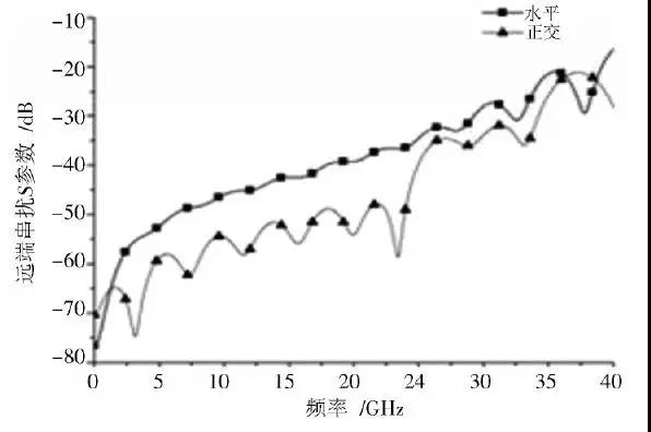
Figure 8 Comparison of differential pair FEXT under different signal distribution methods
From the results shown in Figure 8, it can be seen that when the signals are orthogonally laid out, due to the increase in the distance between the holes and the holes, the coupling between the holes and the holes decreases, and the far-end crosstalk from port D4 to port D2 is lower than that in the horizontal layout. far-end crosstalk. It can be seen from Table 1 that the optimized far-end crosstalk has an improvement of 5-15 dB over the original design in the frequency band greater than 5 GHz. Figure 9 also verifies the superiority of the orthogonal layout from the time domain. The optimized design transient maximum peak noise is 10 mV lower than the original design, as shown in Table 1.

Figure 9 Comparison of differential pair FEXT time domain responses under different signal distribution methods
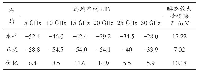
Table 1 Far-end crosstalk comparison
2.3 Number ratio of signal hole/ground hole
Since the spacing of BGA solder joints is fixed in the design, it is impossible to blindly increase the distance between signals to reduce crosstalk. The easiest way is to increase ground hole isolation around important signal holes. The following four schemes have signal hole/ground hole (SG) ratios of 1:1, 1:2, 1:3, and 1:4, respectively, and the signal layout adopts the orthogonal layout in Section 2.2, as shown in Figure 10.
Figure 10 Signal layout of different SG ratios
Figure 11 shows the comparison of the FEXT of the four schemes. When the SG ratio is 1:2, the FEXT of the differential signal is greatly improved compared with the case of 1:1. It can be seen from Table 2 that in the 5~30 GHz frequency band, the SG ratio of 1:2 to the 1:1 far-end crosstalk is reduced by 8~17 dB.
Adding ground hole isolation around important signal holes can shorten the ground return path and reduce the inductance discontinuity of signal vias, so crosstalk can be improved to a certain extent, but it will soon saturate. The SG ratio is 1:4 and 1:1 At 3 o’clock, the difference is not significant, and the improvement of far-end crosstalk is very limited. Figure 12 shows the time-domain simulation results of the far-end crosstalk of the four schemes, and the same analysis results as those in the frequency domain can be obtained. From the time domain results, the transient maximum peak noise of the four schemes can be obtained. When the SG ratio is 1:1, it is as high as 22 mV; when the SG ratio is 1:1, it quickly decreases to 6 mV; when the 1:3 and 1:4 are both at 1.6 mV Left and right, the difference is less than 0.03 mV, as shown in Table 2.
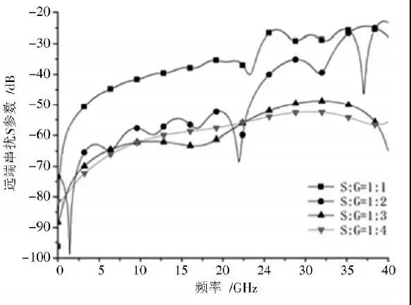
Figure 11 Comparison of FEXT of Four Schemes

Figure 12 Comparison of FEXT time domain responses of four schemes
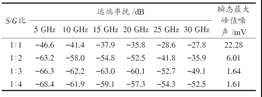
Table 2 Far-end crosstalk comparison
Due to the limited number of pins in the BGA package, the number of ground holes cannot be increased indefinitely. Under the trade-off between the influence of crosstalk and the number of pins, the SG ratio of 1:2 and 1:3 is not much different within 20 GHz, and 1:2 can be selected. Above 20 GHz, the SG ratio of 1:3 is significantly better than 1:2.
2.4 The influence of wiring layer selection and via Stub
Adding ground hole isolation around important signal holes is the easiest way to reduce crosstalk, but it saturates quickly, and it is difficult to achieve an ideal shield. In the package and PCB interconnection area, in addition to the hole-to-hole coupling between high-speed differential pairs, line-to-hole and hole-to-line coupling are also important factors that cause crosstalk. At this moment, in addition to considering the previous three aspects, the impact of wiring layers and via stubs on crosstalk should also be analyzed and studied. In the case of FIG. 13 , three differential pairs are arranged on different layers and have different via stub lengths, the signals are orthogonally laid out, and six isolated ground holes are arranged around each pair of differential vias. The three differential pairs in Figure 13(a) are all laid out on the 10th layer of the PCB, close to the bottom layer. The interference lines on both sides in Figure 13(b) are moved from layer 10 to layer 3, and the long stub is back drilled to 59.1 mil. In this way, the vertical length of the hole-hole coupling between the disturbing signal on both sides and the disturbed signal in the middle is significantly reduced. Figure 13(c) is the opposite of Figure 13(b), the disturbed wire in the middle is laid on the 3rd layer and back-drilled, and the interference wires on both sides are laid on the 10th layer. Figure 13(d) The middle disturbed wire is laid on the 10th layer, and the interference wires on both sides are laid on the third layer and the long stub is reserved.
The frequency domain comparison of FEXT is shown in Figure 14. Compared with scheme (a), scheme (b) reduces the vertical length of the interference signal vias on both sides, reduces hole-hole coupling, and the three pairs of differential lines are not the same The coupling between layers, lines and lines is also reduced, and crosstalk will be greatly improved. It can be seen from Table 3 that in the 5~30 GHz frequency band, the scheme (b) improves the far-end crosstalk by 4~12 dB compared with the scheme (a). The difference between scheme (c) and (b) is that (c) has redundant hole-line coupling, in (c) the disturbed line is placed on the 3rd layer and back-drilled, and the disturbing line is placed on the 10th layer, although the hole-hole coupling It can also be reduced, but the long interference signal holes on both sides will cause hole-line interference to the middle differential line. In scheme (b), due to the back-drilling of the interference signal hole, when the disturbed signal passes through, there is no long stub interference on the differential line. Thus, the crosstalk of option (b) is minimal. If there is no back-drilling, such as scheme (d), although the three pairs of signal differential lines are not on the same layer, the long stub will not only affect the continuity of the impedance, cause the self-differential signal to resonate, but also increase the difference between adjacent differential signals. Crosstalk between them is not even as good as scheme (a) where the signals are placed close to the bottom layer.

Figure 14 Comparison of FEXT of Four Schemes
The same analysis results as in the frequency domain can be obtained from the time domain simulation results, as shown in Figure 15. It can be seen from Table 3 that the transient peak noise of the four schemes, scheme (b) is the smallest, and scheme (d) is the largest. Therefore, in the future design, in order to avoid the interference of the signal by the long Stub of the via hole, the differential line should be routed as close as possible to the bottom layer of the PCB board, and the internal strip line should be used more. Several pairs of parallel differential signals can be arranged on different signal layers to reduce crosstalk, but it should be noted that signal vias on shallow layers must be back-drilled.
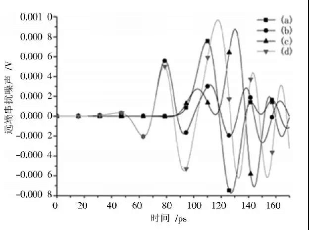
Figure 15 Comparison of FEXT time domain responses of four schemes

Table 3 Far-end crosstalk comparison
3 Comparison and analysis of experimental results
By comparing and analyzing the above simulation results, the following design and optimization suggestions can be obtained:
(1) When the differential signal is drawn from the via hole, in order to meet the requirements of equal length and equal distance, a horizontally symmetrical wiring method should be used as much as possible to achieve the best transmission performance and minimum common mode noise. If absolute horizontal symmetry cannot be achieved when routing, 45° corner routing is better than 90° corner routing.
(2) The signal pin layout of the BGA package adopts an orthogonal method, which can fully reduce the influence of crosstalk between differential pairs. Compared with the horizontal layout, the orthogonal layout has a 5-15 dB improvement in crosstalk in the 5-30 GHz band.
(3) Adding ground hole isolation around important signal holes can improve the crosstalk to a certain extent, but it will be saturated soon. From the simulation results, it can be seen from the simulation results that if 4 ground holes are arranged around each pair of signal holes within 20 GHz, the It can well reduce the crosstalk between differential signals and meet the requirements of signal integrity. Above 20 GHz, 6 isolated ground holes can be placed around some high-speed signals to improve crosstalk between signals.
(4) When selecting the wiring layer, in order to avoid the interference of the signal by the long Stub of the via hole, the differential line should be routed as close as possible to the bottom layer of the PCB board, and the internal strip line should be used. If many pairs of differential pairs are transmitted in parallel, several pairs of differential signals can be arranged on different signal layers to reduce crosstalk, but it should be noted that the differential signal vias arranged in the shallow layer must be back-drilled.
4 Conclusion
In this paper, through the optimal design of the high-speed BGA package and the differential interconnection structure of the PCB, the CST full-wave electromagnetic field simulation software is used to carry out 3D modeling, and the differential wiring method, signal layout method, signal hole/ground hole ratio, wiring layer and via are respectively studied. The specific effects of these four aspects on high-speed differential signal transmission performance and crosstalk.
The time-frequency domain simulation results show that the optimization method can effectively improve the transmission performance of high-speed differential signals, reduce crosstalk between differential signals, and achieve better signal isolation. It provides an important basis for ensuring the signal integrity of the high-speed signal transmission system, and has certain guiding significance for the design of high-speed PCB.