
Shunlongwei Co. ltd.
IGBT Module / LCD Display Distributor
Customer Service
+86-755-8273 2562
IGBT Module / LCD Display Distributor
“Software-defined radio is a new technology that fully combines the advantages of software and hardware that emerged in the 1990s. This technology originates from the special needs of the military field for the flexibility of communication systems. Since software radio was proposed by Joe Mitola in 1992, software radio has been widely used in communication systems. Software radio is an open modular structure, based on a general hardware platform using digital radio (full digital communication transceiver) technology, through real-time software control, users can define the working mode of the platform, so that a The hardware platform can be transformed into a communication system of different technical standards in real time.it is a
“
This design is a general hardware platform implemented for the needs of software radio IF signal processing.
Software-defined radio is a new technology that fully combines the advantages of software and hardware that emerged in the 1990s. This technology originates from the special needs of the military field for the flexibility of communication systems. Since software radio was proposed by Joe Mitola in 1992, software radio has been widely used in communication systems. Software radio is an open modular structure, based on a general hardware platform using digital radio (full digital communication transceiver) technology, through real-time software control, users can define the working mode of the platform, so that a The hardware platform can be transformed into a communication system of different technical standards in real time. It is a new architecture for realizing wireless communication, and its notable features are openness, programmability and fast configurability. This is another major breakthrough in the communication field after analog to digital and fixed to mobile.
Traditionally, the hardware behind the software radio analog front end is mainly composed of the following three parts: high-speed analog-to-digital and digital-to-analog converter, digital up-converter and high-speed digital signal processor. Among them, frequency conversion and signal processing are often implemented in three ways: ASIC, DSP and programmable logic device. Due to the inherent advantages of programmable logic devices in reconfiguration and flexibility, in recent years, some FPGA-based software radio signal processing general platforms have appeared in foreign markets. Such as SANDANCE’s SMT370 development board, NALLATECH’s XtremeDSP development kit and so on. This paper introduces a self-designed and implemented signal processing platform, which is a receiving and testing hardware environment built on the field programmable logic device FPGA for processing.
1.frame
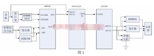
The signal processing platform is composed of high-speed digital-to-analog converter AD6644, high-speed analog-to-digital converter AD9764, xilinx company’s Virtex-4 series FPGA chip XC4VLX25, clock Circuit and regulated power supply circuit. The frame is shown in Figure 1. The analog intermediate frequency signal is provided by the IF signal source, and is input to the FPGA chip after being sampled by AD6644 under the control of the clock circuit. The FPGA performs digital down-conversion and demodulation processing on the digital signal, and then sends it to AD9764 for digital-to-analog conversion, and sends the analog output signal to the oscilloscope for testing. The circuit layout is divided into three areas: the input analog part, the digital signal processing part and the output analog part, so the whole circuit follows the high-speed circuit design principle of analog-digital mixing, adopts an eight-layer circuit board structure, and separates the analog power supply and the digital power supply. The digital power supplies of different voltages are also separated, and the inner layers are correspondingly divided into analog ground, digital ground and analog ground. The three ground layers use ADC and DAC as the junction respectively, and are connected under the chip through magnetic beads or 0Ω resistors respectively.
2.Analog-to-digital conversion circuit design
2.1 Working principle
The AD6644 is an A/D converter with a resolution of 14 bits and a sampling rate of up to 65MSPS. It is capable of converting wideband analog signals with a 100dB spurious-free dynamic distortion range, a typical SNR of 74dB, and a power consumption of 1.3W. It is very suitable for the front-end analog-to-digital conversion of the system.
The AD6644 has complementary analog input pins and . Analog signals use differential inputs. The chip internally encodes the input analog signal by grading, and after each encoding, the size of the analog signal corresponding to the encoded value is subtracted from the total signal, and the remaining signal is sent to the next to obtain 5 bits, 5 bits and 6 bits in turn. After the code is sent to the digital error correction logic for correction, the 14-bit parallel data output is obtained.
2.2 Input circuit
The input of AD6644 is divided into two parts: clock input and analog signal input.
The clock is input from the ENCODE and /ENCODE pins. The sampling clock of AD6644 requires high quality and low phase noise. If the jitter of the clock signal is large, the signal-to-noise ratio is easy to deteriorate, and it is difficult to ensure the 14-bit . To optimize performance, the sampling clock signal of the AD6644 is differential. The clock signal can be AC coupled through a transformer or capacitor to the ENCODE and pins, which are biased on-chip, so no external biasing is required. In this design, a low-jitter clock signal is converted from a single-ended signal to a differential signal with a transformer. Two inverted Schottky diodes are connected at the output of the transformer to limit the amplitude of the clock signal input to the AD6644 to about 0.8V peak-to-peak.
Analog signal from and to input. Two differential input methods, DC coupling and AC coupling, are often used, which is conducive to filtering out even harmonic components, feedback signals of crystal oscillators and interference signals of common mode. The input voltage range of the AD6644 is biased to 2.4V to ground. In transformer coupled mode, the recommended primary to secondary turns ratio is 1:4. Resistive isolation is typically provided between the secondary coil and the AD6644, which limits the dynamic current flow from the A/D device to the secondary coil. In the circuit using operational amplifier coupling, the AD8138 operational amplifier of single-ended-to-differential conversion is usually used, which can reduce the system cost and circuit scale.
3. FPGA circuit design
The XC4VLX25 selected in this design is a chip in the Virtex-4 series for high-performance logic design applications. It contains 24192 logic cells, 10752 slices, 168 distributed RAM and 1296K embedded block RAM.
The Virtex-4 family of devices is configured by transferring application-generated bitstream data to internal memory. Since the configuration memory of XILINX FPGA cannot keep data when power off, it must be configured every time it is powered on.
There are three configuration mode pins M0, M1 and M2 on the chip, through which you can choose among the following configuration modes: serial master mode, serial slave mode, parallel master mode and parallel slave mode, all of which are It is the computer that first loads the data into the PROM chip, and then the PROM chip configures the FPGA. In addition, the bit stream can also be directly processed through the JTAG port, that is, JTAG/boundary scan mode.
Master and Slave modes are determined based on the direction of the configuration clock (CCLK). In master mode, the FPGA generates the configuration clock from the internal oscillator, while in slave mode, the configuration clock pin (CCLK) is an input property. This design uses serial master mode and JTAG mode on the board.
figure 2
The serial master mode only needs a few signals to adapt the interface between the PROM and the FPGA, and does not require an external clock source during the configuration process, so it is also commonly used in various configuration modes that use the PROM. In this mode, the FPGA internally generates the configuration clock. When the /CF pin is at a high level, the data can be obtained from the D0 pin of the PROM, and it is in an enabled state with OE. New data is established a short time after each rising clock edge. The circuit connection is shown in Figure 2.
Another common configuration mode is JTAG mode. A Virtex-4 FPGA can be configured directly with a computer via a JTAG cable while it is powered on. At this point, you only need to connect the corresponding pins of the TCK, TMS, TDI, TDO and JTAG cables of the FPGA chip in the above figure. If this mode is used, M2, M1 and M0 are also set to boundary scan mode accordingly, ie M2=1, M1=0, M0=1.
When designing a circuit board with an FPGA as the center, it should be noted that the input and output signals of the FPGA are high-speed signals. In order to obtain the properties of steep rising and falling edges, the traces should be as short as possible. Therefore, when selecting the corresponding IO for the key signal, select the pins on the periphery of the chip, so that the high-speed signals can be distributed only on the upper signal layer during wiring, and do not need to go through the vias to other layers of the circuit board. Digital signals and analog signals should be routed in areas above their respective ground layers, and ground lines should be added between parallel digital signal lines to eliminate mutual interference.
4. Digital-to-analog conversion circuit design
The AD9764 produced by Analog Devices is a high-speed D/A device suitable for digital-to-analog conversion of FPGA output signals. It features 14-bit resolution, slew rates up to 125MSPS, and a wide spurious-free dynamic distortion range. The differential current output is 2-20mA, and the power consumption is 190mW at 5V and 45mW at 3V, and edge-triggered latching.
4.1 How it works
AD9764 consists of digital and analog parts. The digital part can work on the 125MHz clock frequency, and it includes edge-triggered latching and segmented decoding logic. The analog section includes PMOS current sources, differential switches, a 1.20V voltage reference, and a reference control amplifier.The full-scale output current is adjusted by the reference control amplifier through an external resistor, and its variation range is 2-20mA. The external resistor is connected to the reference control amplifier and the voltage reference Vrefio, which sets the reference current
4.2 Output circuit
The output mode of AD9764 is divided into two types: single-ended output and differential output. In order to facilitate debugging and comparison, these two methods are implemented in the circuit board in this design.
The single-ended output is suitable for those applications that require a unipolar voltage output. When a suitable load resistor Rload is connected between Iouta or Ioutb and the analog ground ACOM, a positive output voltage can be obtained. This method is a good choice for applications that require a DC-coupled ground reference. Usually use the Iouta pin for single-ended output, because this pin has slightly better performance than Ioutb.
In addition to single-ended outputs, the AD9764 uses more differential outputs. Differential output is generally implemented using a transformer or an op amp. The use of a transformer provides suitable distortion resistance for signals whose frequency spectrum is within the passband of the transformer. The transformer can filter out even harmonic components of the signal and noise interference in a wide frequency band, in addition to providing circuit isolation. However, the transformer method can only provide AC coupling. When using an op amp to achieve differential output, the Iouta and Ioutb pins are configured to load two resistors of equal resistance, and then the two voltage signals are differentially input into the amplifier and converted into output signals. Differential operation will help eliminate common-mode error sources associated with Iouta and Ioutb, such as noise, distortion, and DC offset. In addition, the current associated with the differential code and its resulting voltage Vdiff is twice that of the single-ended voltage output, providing twice the signal power to the load.
The author of this article is innovative:
1. Different from the common experimental platform that uses DSP as processing, this design uses FPGA device to process the signal. The whole design takes universality as the consideration, and builds a flexible and configurable processing platform. Based on the development level of FPGA devices, FPGA is used to realize digital signal processing in the application field where PDSP is widely used. Research).
2. Adopting the Virtex-4 series FPGA with powerful DSP processing core newly introduced by XILINX, the application of high-performance DSP can be realized on this chip, which is the expansion of the traditional function of FPGA. In addition, the peripheral input of the chip and the development of the test circuit are completed with the system design standard of high speed and low power consumption, so that the performance of the chip can be exerted.
The Links: LQ190E1LW01 NL10276BC24-21
