Shunlongwei Co. ltd.
IGBT Module / LCD Display Distributor
Customer Service
+86-755-8273 2562
IGBT Module / LCD Display Distributor
Isolated gate drivers require an isolated power supply to generate the
positive and negative voltage rails essential for driving IGBT, SiC or GaN
power modules. Recent advancement in gate driver technology now enable more
compact and efficient inverter designs by integrating advanced control
features, e.g., for secondary side regulation.
Automotive traction inverters using SiC or IGBT power modules typically
require a bipolar gate drive referenced to each power device’s source, isolated
from the low-voltage control circuit. These gate drivers are supplied by small
isolated converters, typically operating from a low-voltage supply (12 V-24 V)
and delivering low-power (1-2 W) bipolar voltages such as +15 V or +18 V and
-5 V, for example.
Common converter topologies include LLC, flyback and push-pull. Push-pull
converters often suffer from poor output voltage regulation, requiring
pre-regulated input voltage, while LLC converters can be complex to design,
especially for a wide input/load range of operation. The latest advancement in
NXP’s GD31xx family of gate
drivers enables efficient power conversion with enhanced control mechanisms,
supporting a broad range of magnetics and operating conditions. With an
external discrete switching MOSFET, the converter can be designed for high
input voltage operation (12 V, 24 V or 48 V for example.) or to supply multiple gate
drivers in a semi-distributed or centralized architecture.
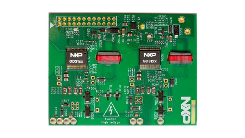
The demonstration platform presented in this article features two gate drivers
from NXP’s GD31xx family, each controlling their own isolated high-voltage
side supplies using onboard planar transformers. The gate drivers ensure
closed-loop operation, providing accurate voltage regulation and fast load
response. Post-regulation is achieved using an LDO for positive voltage and a
shunt regulator for negative bias, ensuring noise-free gate drive and
on-the-fly programmability (see Fig. 2). Typical voltage regulation accuracy
is below 2%, with negative voltage regulation comparable to TL431-like shunt
ICs, while minimizing power dissipation due to the closed-loop operation.

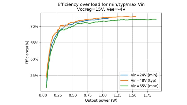
The transformer was designed for 48 V nominal input (24 V – 65 V input range at
full output power) and delivers +15/-4 V outputs at 1 W. This allows for the
driving of approximately 2 µC of gate charge at 20 kHz. The peak efficiency
reaches 74% (see Fig. 3), a reasonable value given the low output power
level, where the gate driver’s quiescent consumption significantly impacts
overall efficiency.
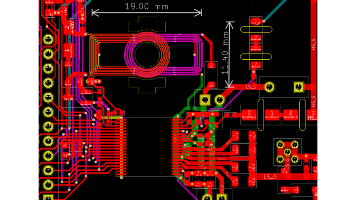
Why are planar transformers considered for such applications? A typical
inverter consists of a vertically stacked configuration of a power module, a
gate driver board, and a control board. Inverter density can be significantly
increased by reducing the vertical spacing between these boards. Since
auxiliary supply transformers are often the tallest components on a gate
driver board, adopting planar transformers minimizes height and improves
mechanical robustness.

Additionally, reducing component height enhances vibration immunity due to the
lower center of mass. In this demonstration platform, the PCB solution
measures just 11 x 19 mm and is less than 5 mm tall, including board thickness
(see Fig. 4). Compared to conventional transformer designs, this resulted in a
threefold height reduction and a 28% improvement in power density.
Transformer design optimization involves balancing leakage inductance, which
impacts efficiency, and interwinding capacitance, which affects common-mode
noise. For this design, a compromise was reached at L
leak
= 5 % L pri and C ww = 4.3 pF by fine-tuning the PCB
stack-up, leveraging varying dielectric thicknesses in this six-layer design.
Hi-pot testing up to 3.5 kV confirms compatibility with the latest SiC and
IGBT power modules.
Despite these benefits, planar transformers are not yet universally adopted.
Some challenges must be considered when integrating these designs into mass
production. While the raw material cost of a ferrite core set may be
attractive compared to conventional discrete transformers, the cost of the
mounting solution must be factored in. Assembly typically involves
adhesives—sometimes reinforced with spring clips—to secure the core halves to
the PCB. This step is critical to ensuring mechanical robustness and
maintaining electrical properties, particularly the final air gap of the core.
Furthermore, achieving the required PCB tolerances and layer stack-up for
proper transformer performance can drive up PCB manufacturing costs. In such
cases, module-based planar transformers may be a more viable alternative,
limiting PCB complexity to the transformer area rather than the entire board.
Planar-based transformer designs for automotive inverter applications offer
significant benefits, enabling designers to further push the boundaries of
power converter density. With advanced control capabilities and high
integration, NXP’s GD31xx gate drivers provide a flexible solution that
accommodates a wide range of transformer designs and power applications across
various semiconductor technologies. This versatility allows engineers to
develop scalable and reusable solutions across multiple platforms, optimizing
efficiency and reliability in modern power systems.