[Introduction]Today, flyback converters are widely used in PoE power supply applications. However, are you still worried about improving the efficiency of PoE power supply? Lightweight and miniaturization is the goal pursued by MPS’ power products. Increasing the switching frequency can reduce the volume of components such as inductors and capacitors. However, as the switching frequency increases, switching losses increasingly become an obstacle to improving efficiency.
Today, the editor will take you to take a look at the culprit of switch loss:
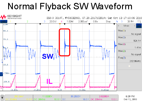
Voltage spikes at turn-off and ringing at turn-on of switching devices
01 Voltage spikes
The voltage spike when the switching device is turned off is mainly caused by the inductance freewheeling, in which the inductance mainly comes from the primary leakage inductance of the transformer and the distributed inductance in the line, and the voltage spike is just released by the energy of the primary leakage inductance. It is caused by the surge of the junction voltage between the source and drain of the switching device.
02 Ringing
The ringing when the switching device is turned on is generated by the resonance of the capacitor and the equivalent inductance. The capacitor is the junction capacitance of the switching device, and the inductance is mainly the excitation inductance of the primary side. The junction voltage of the switching device will keep changing in the resonance state. , so the loss is different at different turn-on moments, and the turn-on loss is usually lower at lower voltages. Of course, zero voltage switching (ZVS) and zero current switching (ZCS) techniques are often used for turn-on losses.
Ordinary PD+DCDC chips mostly use flyback converters as isolated power supplies, and conventional RCD absorption circuits consume leakage inductance energy on resistor R. The more energy is consumed, the lower the voltage stress of the switch tube, but also affects the efficiency of the entire converter. Therefore, there is always a contradiction between the voltage stress of the switching tube and the efficiency of the entire converter in the conventional RCD absorption.

Legend: waveform of flyback converter with RCD absorption circuit
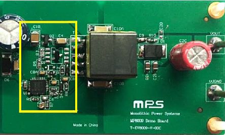
MP8009 is the latest PD+DCDC chip developed by MPS, the internal Pass Device is only 0.48 ohm, the overall efficiency is better, the integration is higher, and it supports 802.3af/at protocol and PSR, SSR, forward, flyback and other topologies structure, and can support active clamp snubber circuit at the same time.

Legend: MP8009 active clamp PSR flyback circuit

Legend: MP8009 Active Clamp PSR Flyback Board
Q: What is an active clamp snubber circuit?
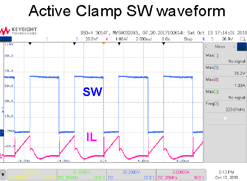
A: Compared with the RCD absorption circuit, the active clamp absorption does not require a resistor to consume energy. Instead, the active clamp circuit is turned on after the switching device is turned off. At this time, the clamping capacitor and the primary side leakage inductance form resonance , absorbs and stores the leakage inductance energy in the first half cycle of resonance, and transfers the leakage inductance energy to the output terminal in the second half cycle. Therefore, the loss is effectively reduced and the converter efficiency is improved.
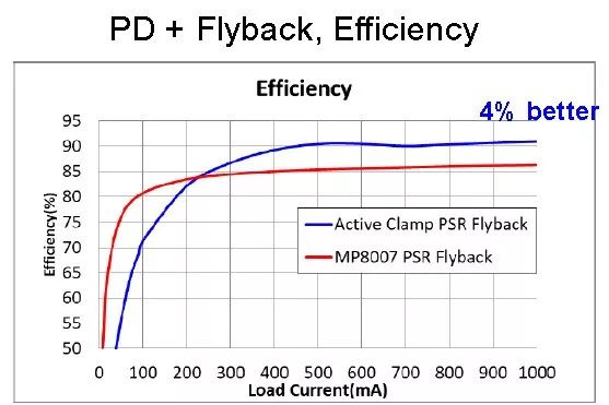
In addition, it also greatly reduces the voltage stress of the switching tube, and finally achieves the most ideal balance between voltage stress and transmission efficiency.

Legend: MP8009 Active Clamp Flyback Converter Waveforms

Legend: Efficiency curve of MP8009 active clamp flyback converter