
Shunlongwei Co. ltd.
IGBT Module / LCD Display Distributor
Customer Service
+86-755-8273 2562
IGBT Module / LCD Display Distributor
Since the invention of the integrated circuit in 1958, integrated circuits have brought immeasurable and huge progress to human civilization. “Laid the foundation for modern information technology” is the pertinent evaluation given to Jack Kilby for his invention of the integrated circuit by the 2000 Nobel Prize in Physics. Today, we can even say: “Integrated circuits laid the foundation for modern technology.” Just imagine, without integrated circuits, to what extent would humankind’s current technology regress?
from time to space
The basic unit of an integrated circuit is the transistor, which I call a functional cell. How to integrate more transistors within a limited area or volume has become the key to the development of integrated circuits. In 1965, Gordon Moore proposed Moore’s Law, which stated that the number of devices on integrated circuits would double every eighteen months, predicting the development of integrated circuits in terms of time. In human cognition, time and space are inseparable, and we often call them time and space. Time has one dimension, and space has three dimensions, collectively called four-dimensional space-time. Time is one-way and can only develop forward, while every dimension of space can develop in both directions. When the development of things is limited or constrained by time, they will look for breakthroughs in space. It is called exchanging space for time. This is also the case with the development of integrated circuits.
In Moore’s Law, we focus on the exponential increase in the number of transistors over time. As Moore’s Law becomes unsustainable, today’s integrated circuits focus more on how to manufacture more transistors in a limited space.
The only way to 3D: Space has three dimensions and six directions. If you want to integrate and manufacture more transistors in a limited space, you must exhaust all three dimensions and six directions. Since the invention of integrated circuits, transistors have been fabricated and interconnected on the plane of a wafer. In order to manufacture more transistors in a limited area, the size of the transistors needs to be made smaller and smaller, until one day, when the planar transistor shrinks and can no longer work properly, a new type of transistor, FinFET, replaced the planar transistor, and later developed GAA transistors, both of which belong to the 3D structure of transistors, are called the first level of 3D in 3D-IC. 3D transistor structure does not completely solve the problem, so the second level of 3D in 3D-IC has also appeared, that is, transistor stacking, the more representative one is CFET.
At the same time, people have found that in advanced packaging, stacking chips can also effectively increase the integration density of transistors, that is, integrating more transistors in an effective space. This is the third level of 3D in 3D-IC. For urban development, if we want to increase the residential density of the city, we need to build high-rise buildings. For integrated circuits, to increase the integration density, 3D integration must be adopted. Next, we will analyze the three levels of 3D in 3D-IC one by one.
3D level 1 3D rendering of transistor structures
The transistors used in integrated circuits are usually Field-Effect Transistors, referred to as FETs. The initial form of the gate of this type of transistor is planar and is called a planar transistor Planar FET. Its characteristic size (Feature Size) refers to the width of the gate (Gate Width), that is, the channel length (Channel Length) of the MOS device.
As the size of the transistor gradually shrinks, its characteristic size also continues to shrink. When the characteristic size reaches 22nm, the planar transistor has a short channel effect due to its gate’s weak control ability over the channel, and is gradually being replaced by a new type of transistor. Replaced by Fin Field Effect Transistor (Fin FET). At this time, the feature size no longer uses the width of the gate as its measurement standard, but represents the equivalent size of the transistor density in this process compared with the previous generation process. For example, for a chip with the same area, the number of transistors is doubled. At this time, the characteristic size of the transistors of this chip is 0.7 of the characteristic size of the previous generation, and so on. Of course, different semiconductor manufacturers have different definitions of feature size. For example, the definitions of Intel and TSMC are not exactly the same. From the planar transistor Planar FET to the fin transistor FinFET, it is a major change in the transistor structure. The internal structure of the transistor moves from plane to 3D. We call it the 3Dization of the transistor structure. At 3nm, Fin FET’s ability to control current is somewhat inadequate, so it is necessary to use stacked nanosheet transistors GAA FET. GAA uses a structure in which the gate surrounds the channel. The gate’s ability to control the channel is enhanced compared to Fin FET, allowing the transistor to achieve better performance in a smaller space. The picture below shows a comparison of the microstructure of three transistors: Planar FET, Fin FET, and GAA FET.

The following figure is a structural comparison of three types of transistors manufactured in parallel with NMOS transistors and PMOS transistors. The most common basic unit of an integrated circuit is usually composed of NMOS transistors and PMOS transistors.

Currently, in advanced processes, Fin FET is the mainstream, GAA FET is catching up from behind, and is expected to fully replace Fin FET after 3nm, while Planar FET continues to exert its waste heat in large-size devices.
3D Level 2 3D Integration of Transistors
From the above description, we can see that the transistor structure of today’s mainstream chips has been fully 3D.
In a chip, transistors are just a thin layer. Is it possible to make multiple layers of transistors, stacking them on top of each other? This is what we are going to talk about below: the stacking of transistors, that is, the 3D integration of transistors.
With the continuous development of Moore’s Law, the chip manufacturing process is getting closer and closer to the physical limit. In order to further increase the number of devices per unit area, the industry began to try to stack transistors that achieve a 3D structure, and proposed CFET using vertically stacked transistors.
CFET
CFET complementary field effect transistor is regarded as a key element of the process below 1nm. It is a new generation of transistor technology after FinFET and GAA.
The following figure is a structural comparison of GAA FET and CFET. It can be seen that in GAA FET, the NMOS tube and PMOS tube are placed side by side and on the same plane, while in CFET, the NMOS tube and PMOS tube are stacked vertically, and the NMOS tube is located above the PMOS tube. , its area footprint is only half that of GAA FET.
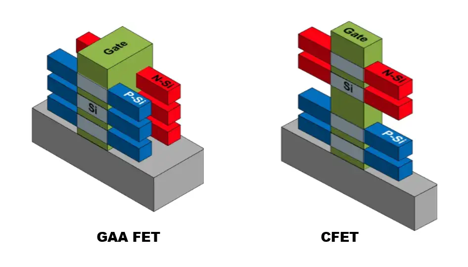
Therefore, the area of a chip using a CFET vertical stacking architecture can be reduced by up to 50% compared to a chip using a GAAFET architecture.
The figure below shows a cross-section of the CFET transistor layer, with the NMOS tube above the PMOS tube.

CFET combines PMOS transistors and NMOS transistors, making the switching speed and driving capability complementary, thus improving the overall performance of the transistor. CFET allows the industry to see new development prospects for transistor structures. At present, the CFET manufacturing process needs to solve a large number of technical challenges brought by multi-layer transistor stacking. It is conservatively estimated that it will take 8-10 years for the CFET structure to be put into commercial use. From now on, we will have to wait and see whether more layers of transistors can be stacked on top of CFETs.
3D Level 3 3D Integration of Transistor Groups
In this article, I use a new term, Transistor Group, which refers to the general name of the transistors in a chip completed under a specific process. For example, all transistors in an SoC form an SoC transistor group, and all transistors in a Chiplet form a Chiplet transistor group. Groups of transistors are typically manufactured in one go using the same process. In a chip, the volume occupied by the transistor group and its interconnections is what I call the effective functional volume (EFV). Compared with the volume of the entire chip itself, the proportion of the effective functional volume is not large. . Through wafer thinning and then 3D stacking, the proportion of effective functional volume can be increased, thereby improving the functional density of the system. The figure below shows a comparison between SoC and SoIC, where red is the volume occupied by the transistor group and yellow is the chip volume. The SoC contains 1 transistor group, and the SoIC contains 3 transistor groups.
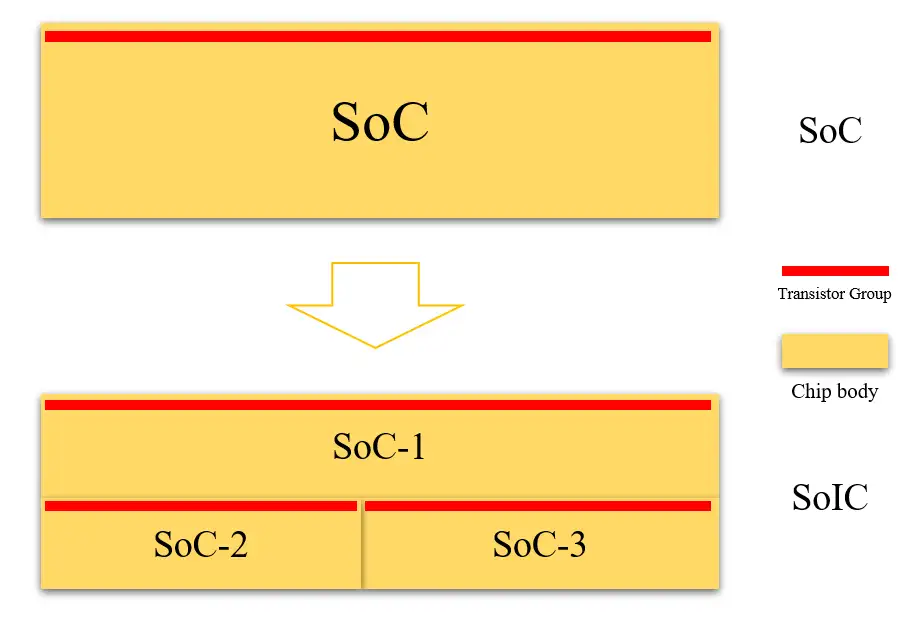
It can be seen that under the same volume, the three transistor groups in the SoIC occupy a larger proportion of the volume, and their effective functional volume EFV is larger. Therefore, under the same process, the functional density of SoIC is higher, that is, more transistors can be integrated in the same volume. At the same time, the three transistor groups in the SoIC can be manufactured using different process nodes, so it is more flexible.
3D integration of transistor groups is the most popular technology in integrated circuits today. Some people call it 3DIC, some call it advanced packaging, and some call it Multi-Die or SiP technology.
The figure below shows a screenshot of a typical HBM advanced package design in an EDA tool.

Summarize
From the 3Dization of transistor structures to the 3D integration of transistors to the 3D integration of transistor groups, there are three levels of 3D, which complement each other and do not conflict. The ultimate development goal is to achieve 3D at all three levels. The first level of 3D, the 3D transistor structure has been realized through FinFET and GAA. According to the needs of different process nodes, Fin FET, GAA FET or Planar FET can be flexibly used. The second level of 3D, 3D integration of transistors, that is, transistor stacking, has been demonstrated to be possible through CFET. However, due to the large technical challenges in its process, it will take 8-10 years to achieve commercial use. The third level of 3D, 3D integration of transistor groups, can be achieved through advanced packaging technology. The current 3DIC mostly refers to this category. Advanced packaging requires stacking and interconnecting the transistor groups through wafer thinning, TSV, RDL, Hybrid bonding and other technologies after the transistor group is manufactured. Currently, its key technologies are TSV, Hybrid bonding, etc. From the 3Dization of transistor structures to the 3D integration of transistors (transistor stacking) to the 3D integration of transistor groups (transistor group stacking), three levels of 3D create the ultimate 3D-IC.


