Content last revised on October 16, 2026
Benchtop Waveform Tuning: Mitigating Stress by Damping Tail-Current Oscillations During Turn-On of BSM150GAL120DN2
Check the switching node with a properly rated differential probe before changing the gate network. In an industrial inverter welder or medium frequency induction heating supply, a long diode recovery tail, excessive reverse recovery current, or a sharp current rebound can appear as overshoot, ringing, unexpected electromagnetic noise, and abnormal heating around the commutation loop.
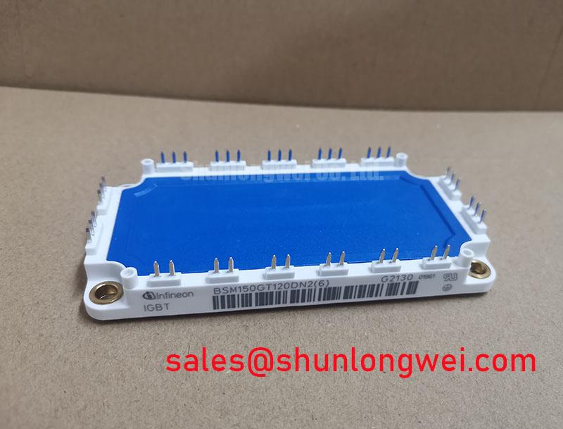
BSM150GAL120DN2 is an Infineon IGBT module with an official rated voltage of 1200.0 V, an official rated current of 150.0 A, and a Module package. These are device identification and rating values, not a complete operating envelope for a finished converter. Junction temperature, switching frequency, pulse duration, cooling conditions, gate drive behavior, commutation topology, and load current must be evaluated together.
During bench tuning, capture collector emitter voltage, gate emitter voltage, and commutation current on the same time base. The antiparallel freewheeling diode can produce a reverse recovery peak identified as Irrm. A high reverse recovery slope, often described as a snappy recovery event, can interact with stray inductance and create a voltage spike at the IGBT terminals. The correct response is to separate the source of the ringing from the effect: compare the gate waveform at the module terminals with the driver output, then compare the measured switching node with the current transition.
An engineering recommendation is to begin with the existing gate resistance and change only one element at a time. A modest increase in turn on resistance may reduce current slew rate and soften diode recovery interaction, but it can also increase switching loss. A gate network that appears stable at light load may behave differently at the production current of an inverter welder or induction heating stage. The final value is therefore system determined and should be selected from measured switching loss, peak voltage, current sharing, and thermal results.
RC snubber evaluation should follow the actual ringing frequency and energy observed at the switching terminals. The snubber loop should be physically compact, with its return path kept close to the high di/dt commutation path. Avoid routing the gate return beside the power switching loop, and maintain practical clearance from copper areas carrying fast voltage transitions. Snubber leads that are long or looped can add enough parasitic inductance to reduce the intended damping effect.
When a waveform changes after the probe ground or probe position is moved, treat the measurement arrangement as part of the circuit. Use a differential probe with an appropriate common mode rating and keep the probe connection short. Confirm the result with a known good switching position or a low energy test condition before adjusting the production gate drive.
Transient Dynamics and Electrical Design: Coordinated Protection for the IGBT Module
Coordinated semiconductor protection requires the semiconductor fuse clearing behavior and the module short circuit withstand capability to be assessed as one protection system. The 1200.0 V voltage rating and 150.0 A current rating identify the BSM150GAL120DN2, but they do not by themselves define the correct fuse, allowable overload profile, or short circuit interruption result.
For a DC link fault, compare the selected high speed fuse total clearing I2t with the module’s applicable short circuit and thermal limits from the component documentation and the converter protection study. The fuse must interrupt the fault before the semiconductor and its internal connections are exposed to destructive energy. The analysis should include prospective DC link current, bus impedance, fuse pre arcing behavior, total clearing time, gate shutdown delay, and the physical distance between the fuse, capacitor bank, and module.
A gate driver fault response also affects coordination. A desaturation or overcurrent protection circuit may command the IGBT off, but the driver delay, soft shutdown profile, isolation behavior, and fault latch sequence determine how much energy remains in the circuit. Verify that the driver does not repeatedly restart a faulted leg, and inspect the gate emitter voltage during the full protection event rather than only during normal switching.
Diode reverse recovery can increase the first current peak during a hard commutation fault. This is one reason the protection assessment should include the freewheeling path, not only the IGBT. A snubber can reduce ringing energy at the switching node, while a carefully tuned gate network can moderate the turn on transition. Neither measure replaces a coordinated fuse and fault interruption design.
For an industrial inverter welder, inspect the weld current control loop and fault handling sequence together with the semiconductor protection. For medium frequency induction heating, also review the resonant network, load detuning behavior, and capacitor fault response. These applications can present different current waveforms even when the same module rating is used.
| Item | BSM150GAL120DN2 | Reference component |
|---|---|---|
| Manufacturer | Infineon | BSM100GT120DN2 |
| Rated voltage | 1200.0 V | Confirm from the reference component documentation |
| Rated current | 150.0 A | Confirm from the reference component documentation |
| Package | Module | Confirm mechanical compatibility before substitution |
The linked reference model should be treated as a separate device identity, not as an automatic replacement. Before evaluating any interchange, compare terminal arrangement, electrical ratings, switching characteristics, gate requirements, thermal interface, mounting geometry, isolation behavior, and the original equipment protection settings. A mechanical fit alone does not establish electrical compatibility.
Maintenance Note: De energize and discharge the DC link before touching the module terminals, then check heatsink contact condition, airflow blockage, and terminal tightness during scheduled maintenance.
Transient Dynamics and Electrical Design: DC Link Capacitance Bank Layout and Low ES for BSM150GAL120DN2
Place the DC link capacitance and the BSM150GAL120DN2 commutation path according to current flow, not cabinet convenience. The objective is to minimize parasitic loop inductance so that the voltage generated during a rapid current transition remains within the verified peak voltage margin of the switching device and the complete power stage.
The relationship between switching voltage and stray inductance can be considered in the form of a DC link voltage term plus an inductive term produced by loop inductance and current slew rate. This is an engineering calculation principle, not an additional factory rating for the module. The practical task is to measure the peak at the module terminals and compare it with the actual DC link condition across operating temperature, load current, and switching state.
A low impedance capacitor bank should present a short, symmetrical path to the upper and lower power terminals. Keep the positive and negative bus conductors closely coupled where the insulation system permits, and avoid narrow necks, unnecessary bends, and long branch connections. Symmetrical planar busbar geometry can reduce current imbalance between parallel paths, but the finished assembly still requires verification for temperature rise, clearance, creepage, mechanical stress, and insulation coordination.
Snubber capacitor placement matters as much as its nominal capacitance. A component mounted far from the module may damp a cabinet level resonance while leaving the local collector emitter overshoot largely unchanged. Measure at the module power terminals, inspect the snubber current path, and compare the waveform with the snubber connected and disconnected only under controlled, low energy test conditions.
Low ESR capacitors can reduce high frequency voltage movement, but capacitor selection must also consider ripple current, temperature, service life, voltage sharing, discharge behavior, and failure containment. The capacitor bank should be reviewed as part of the full DC link, including precharge, discharge, fusing, busbar insulation, and the physical location of the switching bridge.
When a long motor cable connects the inverter to the load, reflected wave behavior can raise the voltage seen at the motor terminals and alter the current transition at the inverter. The appropriate filter, cable arrangement, common mode treatment, and switching profile are system decisions. Verify both ends of the cable with suitable measurement equipment and check the result against the module terminal waveform rather than assuming that a motor side symptom originates inside the IGBT module.
Gate drive dead time should be established from the actual turn off and turn on behavior of the paired devices, including driver propagation delay, temperature variation, load current, and diode recovery. Excessive dead time can increase diode conduction and recovery stress, while insufficient dead time can permit cross conduction. The final setting should be validated during switching tests and protection tests for the completed bridge.
For broader implementation work covering gate drive interaction, thermal management, commutation layout, and circuit topology, consult the IGBT Design and Integration guide. Infineon’s IGBT Modules and Discretes Official Portfolio provides manufacturer portfolio context, while the Infineon TRENCHSTOP IGBT3 application note discusses relevant high speed IGBT switching behavior. Use those technical references alongside the specific component documentation and the measured converter waveform.