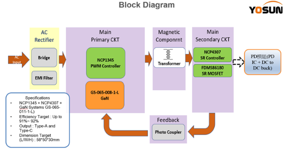
UNGA Holdings recently announced that itsYoushang launched a 65W PD power solution based on Onsemi’s NCP1345 controller and GaN System GS-065-011-1-L power transistor.

Figure 1-The display board of the 65W PD power solution based on Onsemi and GaN System products
As the charging power of mobile devices continues to increase, miniaturization and portability of high-power chargers will become important development directions in the future. In the past cognition, power is often inseparable from the size of the charger. Generally speaking, the larger the output power, the larger the size. However, with the use of GaN power devices, chargers with both high power and compact appearance have become possible. The 65W PD power solution based on onsemi’s NCP1345 and GaN System products launched by the Great United Friends of the United Nations meets the market’s demand for PD fast charging sources.

Figure 2-The display board of the 65W PD power solution based on Onsemi and GaN System products
NCP1345 is a highly integrated quasi-resonant Flyback controller, suitable for many types of high-performance power converters. In terms of design, it uses a dual VCC architecture that allows direct connection to the auxiliary winding to simplify the number of VCC management devices and increase performance.

Figure 3-The display board of the 65W PD power solution based on Onsemi and GaN System products
NCP1345 also has an output limit Circuit based on the primary side to ensure that the constant output current limit can be maintained regardless of the output voltage or output power. Not only that, the quasi-resonant (QR) proprietary valley locking circuit of NCP1345 can ensure stable valley switching. When it drops to the 6th wave trough, the controller will enter the frequency reduction mode to reduce the switching loss. And as the load decreases further, NCP1345 enters SKIP mode to manage power. In addition, in order to ensure the safety and durability of the power supply, NCP1345 has built-in Brown out/in detection, overvoltage protection, overtemperature protection, and AC line voltage removal detection functions.

Figure 4-The display board of the 65W PD power solution based on Onsemi and GaN System products
This solution also uses GaN System’s GaN FET: GS-065-011-1-L (650V/190mohm/5X6) as the main power conversion, with a new generation of synchronous rectification IC NCP4307, no need to supplement additional components, you can Complete the synchronous rectification function.
In order to further optimize the flexibility of practical applications and quickly meet the needs of different customers and markets, the solution adopts the design of power module (AC to DC) + PD module (PD IC + DC to DC buck), which can correspond to different PDs The output interface, without changing the power supply module, can meet the design needs with random matching, which greatly reduces the RD development cycle.
Core technical advantages:
● Integrated high voltage starting circuit and BO/I detection;
● Integrated X2 capacitor discharge function;
● Wide VCCL range: from 8V to 38V;
● 150V VCCH pin, used to connect to the high-voltage auxiliary winding;
● 36.5V VCC overvoltage protection;
● Based on the constant output current limit of the main side;
● Abnormal overcurrent fault protection of winding short circuit;
● IC internal temperature protection;
● The trough switching operation and trough locking are the reduction of noise;
● Fast frequency reduction, used to quickly reduce switching loss;
● Skip mode with output voltage compensation;
● Minimize no-load power consumption;
● Reduce the frequency jitter of EMI;
● Lock or automatically restore overload protection;
● Adjustable over power protection;
● Fixed/adjustable maximum frequency operation;
● The designated pin is the setting of the fault condition and OTP is compatible with NTC.
Scheme specifications:
● Input characteristics:
※ AC input voltage level: 100VAC to 240VAC;
※ AC input voltage range: 90VAC to 264VAC;
※ AC input frequency: 47HZ to 63HZ.
● Output characteristics:
※ Output voltage: +21.0V;
※ Output tolerance: +/-1.0V;
※ Minimum load current: 0A;
※ Maximum load current: 3.25A;
※ Line adjustment: 1%;
※ Load regulation: 5%.
Key words:
‘); (window.slotbydup=window.slotbydup || []).push({ id: ‘3303971’, container: s, size: ‘20,5’, display:’inlay-fix’ }); })();