
Shunlongwei Co. ltd.
IGBT Module / LCD Display Distributor
Customer Service
+86-755-8273 2562
IGBT Module / LCD Display Distributor
“In some special industrial occasions, it is sometimes necessary to collect and store the signal of the sensor continuously in real time, and then play back the data to the PC for analysis and processing after a certain period of time. In the case of harsh working environment, the solution of using high-performance single-chip microcomputer and industrial-grade large-capacity FLASH memory is probably the most appropriate choice.
“
In some special industrial occasions, it is sometimes necessary to collect and store the signal of the sensor continuously in real time, and then play back the data to the PC for analysis and processing after a certain period of time. In the case of harsh working environment, the solution of using high-performance single-chip microcomputer and industrial-grade large-capacity FLASH memory is probably the most appropriate choice. C8051F320 SOC of CYGNAL Company is a kind of high-performance one-chip computer with 8051 core, the running speed is 12 times of ordinary 8051. The chip’s internal 528-byte random RAM and 2048-byte XRAM provide ample space for data buffering and program execution. What is more popular is that its serial expansion function provides great convenience for the expansion of various serial chips and external device interfaces. The seamless connection between the high-speed SPI hardware interface and the serial FLASH RAM greatly simplifies the circuit board wiring, and the built-in USB interface function makes data storage and playback very simple and fast. With the support of the USB interface protocol, the data playback process of the acquisition and storage circuit is extremely simple.
This paper presents a data acquisition and storage circuit for large-scale photovoltaic system operation status monitoring. Due to the surface mount technology, the width of the entire circuit board is only 18 mm, which is as convenient as using a U disk.
Acquisition circuit hardware part
The hardware structure of the circuit
This system adopts C8051F320 chip of CYGNAL Company and AT45DB321C memory chip of ATMEL Company as the main chip of control and storage. Figure 1 is a block diagram of the acquisition and storage system of the signal acquisition system.
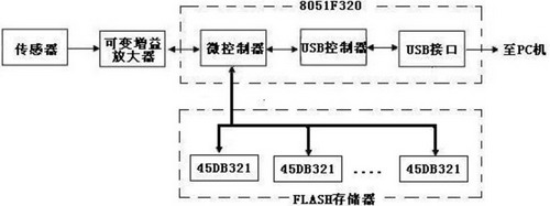
Figure 1 Block diagram of USB-based data acquisition and storage system
As can be seen from Figure 1, during the acquisition process, the input analog signal of the sensor is amplified by the variable gain amplifier and sent to the C8051F320, which is converted into a digital signal through the ADC. There are 8 45DB321C chips outside the single chip to form a 32MB Data flash memory, and the collected data are continuously transmitted to the 45DB321C chip for storage through the SPI interface.
Compared with other types of chips, the C8051F320 has a USB interface, and the on-chip USB function control module conforms to the USB2.0 specification, which can run at full speed or low speed, and has a 1KB USB cache, an integrated transceiver, and no external resistors are required. Can be plug and play with PC. When the data is needed, the acquisition and storage circuit can be retrieved from the site, played back to the PC through the USB interface, and the waveform Display and data analysis and processing are performed on the LabVEIW platform.
The hardware interface of 8051F320 and 45DB321C
In the system, C8051F320 and 45DB321CI use SPI single master and multiple slaves to communicate. The pin NSS is used as the slave selection line to select the memory chip, and the low level is active; SCK is used as a synchronous clock signal for the serial peripheral interface to send and receive data; RDY/BUZ is used to judge whether the device is not busy or ready to receive new command operations. Signal line; SO, SI as data transmission line.
The design of this system considers the use of 8 45DB321C chips with a maximum capacity of 32MB, which are respectively connected to the CS terminals of each 45DB321C through chip selection CS1~CS8. The clock SCK is only valid for the selected 45DB321. In addition to providing sufficient storage space, the design of this system using multiple Flash chips also solves a key problem, which is to learn from the idea of RAID technology in the field of hard disks, and realize a basic parallel acceleration by sequentially operating a group of 4 Flash chips. , Solve the problem of slow writing speed of Flash, and greatly improve the storage performance.
The specific circuit is shown in Figure 2, in which the SPI of 8 pieces of memory is only drawn by cascading, and the respective CS chip selection signal is given by 74HC138 decoding.
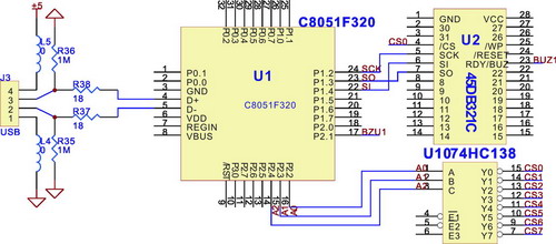
Figure 2 The interface circuit between the single-chip microcomputer and the FLASH memory
Program software for acquisition circuit
The program of the acquisition circuit refers to the program solidified in C8051F320, which is written in C language and consists of four parts: the main program module, ADC data acquisition, Flash data storage and USB communication.
Main program and ADC data acquisition
The main program mainly completes the system initialization state indication operation control and parameter setting to start A/D conversion, etc.
The ADC data acquisition program converts the analog signal from the sensor to a digital signal. In this system, the conversion of ADC is triggered by the automatic overflow of Timer2, and the acquisition rate can be set by the host computer in advance.
Flash data storage program
The communication between C8051F320 chip and Flash memory adopts SPI interface, and the data transmission rate is 12MHz (bit/second). In this design, C8051F320 works in SPI master mode, and the data transmission of SPI bus will be initiated by C8051F320. Firstly, configure the SPI related SFR SPI0CFG register and SPI0CN register to make it work in 3-wire master mode at 12MHz. When communicating, firstly use the GPIO pin to select the corresponding Flash slave device, and then read and write by reading the SPIDAT. When using the Flash chip for read and write operations, the state of the Flash memory must be determined first. By writing the D7H command, read the status register to determine whether the device is Ready or Busy. After the status is determined, related read, write and erase operations can be performed according to the command format in the data sheet.
USB communication program
Firmware programming is a major part of the USB device development process. The main task of the firmware is to initialize the microcontroller and peripherals, send USB requests, and respond to the host’s standard device requests. Complete various data exchange requests according to the functional classification of the device. The initialization programming mainly completes the initialization of the USB controller, the endpoint initialization, the crossbar and I/O port initialization, the system clock setting, and the controller enabling. After initialization, the USB device can be inserted into the host at any time, and the host will follow the USB protocol to identify and initialize the device. After the host recognizes the device, it configures the device, calls the corresponding driver, and performs related communication operations with the host computer software.
Silicon lab offers a development kit for USBXpress. By using the USBXpress library, the development of USB firmware programs and PC-side drivers is greatly simplified. USBXpress implements the application programming interface (API) on the microcontroller side through a series of functions. These functions encapsulate the details of the USB protocol, so that program developers can use USB for data communication without knowing too many details of USB (see Figure 3).
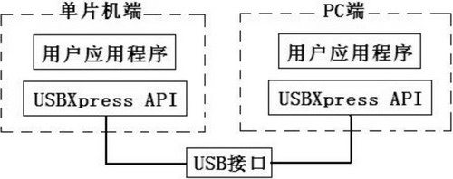
Figure 3 USB communication between single-chip microcomputer and PC
The four functions of initialization, read, write and interrupt are mainly used in this system:
Initialize USB_Init(0,0xEA61,NULL,NULL,Serial,250,0×80,0×100) function; block write function Block_Write(); block read function Block_Read(); USB interrupt enable function.
All handling of the USB is done through the USB’s Interrupt Service Routine. After entering the USB interrupt, the program calls the Get_Interrupt_Source() function to obtain the entry reason of the USB interrupt. Then according to different entry conditions, the corresponding processing is carried out. For example, after receiving the data, read the corresponding buffer content into the memory; when receiving the initialization command, reset each state parameter in the microcontroller. The flow chart of USB communication is shown in Figure 4.
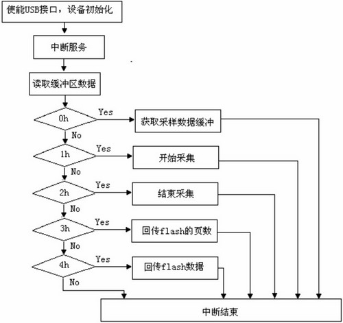
Figure 4 USB communication flow chart
PC software program
The computer software program includes two parts: USB driver and user application.
USB driver
A USB driver is a software component that encapsulates the functions of an application program to access hardware devices. Some devices have the same properties, and they are grouped into a set of standard classes, and the device class specification can be defined as the host driver framework for this class of devices. Device class drivers use similar functions to handle the communication between different devices, so that the development of device class drivers can be separated from the device manufacturer.
The USB driver model is generally divided into five layers (see Figure 5).
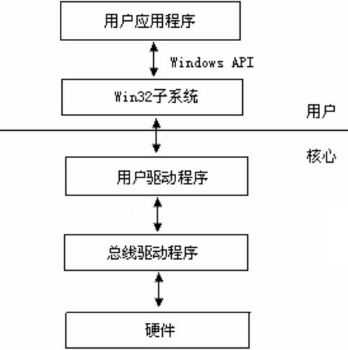
Figure 5 USB driver model
If the client wants to read data from the device, it will call an application program interface API, such as OpenFile, SiUSBXp.dll implements this API. The bus driver controls access to all devices on the bus.
In this system, USBXpress Development Kit is used to develop USB device driver. The main functions are as follows:
SI_Open() function; SI_Close() function; SI_Read function; SI_Write() function; SI_GetNumDevices() function; SI_CheckRXQueue() function.
User application
In this system, the application program is written by the LabVIEW software of NI company, and the software is developed by using the graphical C language to realize the display of data, the analysis function to meet different needs and the parameter setting of the data acquisition hardware (see Figure 6). .
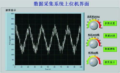
Figure 6 Playback data waveform display interface
Epilogue
The acquisition and storage circuit based on C8051F320 USB interface closely combines computer technology with traditional signal acquisition technology, and fully utilizes the respective advantages of PC and single-chip microcomputer to realize the acquisition, storage, display and processing of sensor signals. With the help of the communication function of the USB interface, the complexity of the data transmission system is reduced.
The Links: FZ400R12KS4 2MBI150NC-060


