
Shunlongwei Co. ltd.
IGBT Module / LCD Display Distributor
Customer Service
+86-755-8273 2562
IGBT Module / LCD Display Distributor
“Wafers are one of the important components of technology. Without wafers, advanced technology will stop moving forward. So, after the wafer is manufactured, how to determine the quality of the finished wafer? In this article, the editor will introduce the testing method of the wafer and discuss the shape change of the wafer.
“
Wafers are one of the important components of technology. Without wafers, advanced technology will stop moving forward. So, after the wafer is manufactured, how to determine the quality of the finished wafer? In this article, the editor will introduce the testing method of the wafer and discuss the shape change of the wafer.
1. Wafer material
Silicon is refined from quartz sand, and the wafer is purified by silicon (99.999%), and then these pure silicon are made into silicon crystal rods, which become the material of quartz semiconductors for manufacturing integrated Circuits. After photoengraving, grinding , polishing, slicing and other procedures, the polycrystalline silicon is melted and pulled out of the monocrystalline silicon ingot, and then cut into thin wafers.

2. Wafer test method
The wafer test is a needle test for each die on the wafer. A probe as thin as a hair made of gold wire is installed on the detection head, which is in contact with the contacts on the die to test its electrical characteristics. The dies will be marked, and then when the wafer is cut into individual dies in units of dies, the unqualified dies marked with the marks will be eliminated, and the next process will not be performed, so as to avoid unnecessary increase in manufacturing costs.
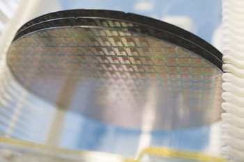
After the wafer fabrication is completed, wafer testing is a very important test. This step of testing is a transcript of the wafer production process. During the test, the electrical capability and Circuit function of each chip are detected. Wafer testing is also known as chip testing or wafer electrical testing.
During testing, the wafer is held on a vacuum chuck and aligned with a thin probe electrometer while the probe contacts each of the chip’s bond pads (Figure 4.18). The electrical tester tests the circuit under the drive of the power supply and records the results. The number, order and type of tests are controlled by a computer program. The tester is automated, so no operator assistance is required for testing after the probe probes are aligned with the first wafer (either manually or using an automated vision system).
The test is for the following three goals. First, qualified chips are identified before the wafers are sent to the packaging plant. Second, the electrical parameters of the device/circuit are characterized for evaluation. Engineers need to monitor the distribution of parameters to maintain the quality level of the process. Third, the accounting of qualified and defective chips will provide feedback on overall performance to wafer production personnel. The positions of good chips and defective products on the wafer are recorded on the computer in the form of a wafer map. The old technology of yesteryear smears a dot of ink on the defective chip.
Wafer testing is one of the main statistical methods of chip yield. As the chip area and density increase, the cost of wafer testing is increasing. As a result, chips require longer test times and more sophisticated power supplies, mechanisms, and computer systems to perform tests and monitor test results. Visual inspection systems also become more sophisticated and expensive as chip size increases. Chip designers are required to introduce test patterns into memory arrays. Test designers are exploring how to simplify the test process more efficiently, such as using a simplified test procedure after chip parameter evaluation is passed, and testing chips on a wafer interlaced, or testing multiple chips at the same time.
3. Wafer shape change
1. Why are wafers round?
Because the production process determines that it is round. Because the purified high-purity polysilicon is spin-grown on a seed. After the polycrystalline silicon is melted, put it into a crucible (Quartz Crucible), and then put the daughter crystal into the crucible and rotate it at a constant speed and pull it upward, then the molten silicon will grow into a cylindrical silicon ingot (ingot) along the daughter crystal direction. . This method is the CZ method (Czochralski), also known as the single crystal Czochralski method, which has been used now. As shown below:

Then the silicon ingot is cut into a silicon wafer by diamond wire:

After grinding and so on, the subsequent processes can be carried out (one of those things that CPU manufactures: i7 and i5 are actually twin brothers!?)
Rotary pulling in the single crystal Czochralski process determines the cylindrical shape of the ingot and thus the circular shape of the wafer.
2. Why is it not round again later?
Then why is it not round again? In fact, there is a process in the middle, that is Flat/Notch Grinning.
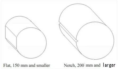
It takes place after the ingot is made. On silicon ingots below 200mm, a flat angle is cut, called Flat. On silicon ingots above 200mm (inclusive), in order to reduce waste, only a small circular mouth is cut, called Notch. After slicing the wafer becomes like this:

The wafer actually lacks a small gap.
Why do you want to do this? Isn’t this a waste? In fact, this small gap is too close to the edge and is very small. It is doomed to be useless when making Die. This can help the subsequent process to determine the placement of the Wafer. For positioning, also The crystallographic orientation of single crystal growth is indicated. The positioning device can be like this:

It is more convenient to cut and test in this way.
The Links: QM200DY-H 2SB0710ARL


