


Content last revised on September 10, 2026
Preventing Spurious Faults: Static and Dynamic Current Distribution Guidelines for QM200DY-H
When several power paths operate in parallel, current distribution must be checked in both the steady state and during switching transitions. A positive temperature coefficient of the on-state voltage can support steadier static sharing in suitable operating regions, but the result depends on device matching, thermal coupling, base-drive symmetry, and the actual operating point. This is a Design Consideration, not a model-specific guarantee unless confirmed by the applicable Mitsubishi Electric documentation.
For a commercial string inverter or micro-grid energy storage converter, keep the collector and emitter power paths physically symmetrical wherever parallel operation is being evaluated. Each path should have comparable conductor length, contact resistance, loop area, and thermal environment. Avoid allowing one module to sit directly in the preferred airflow while another operates in a recirculation zone. A current probe or calibrated shunt arrangement should be used during commissioning to compare branch current under startup, steady load, regeneration, and battery charge or discharge transitions.
Dynamic imbalance is often more visible in the base-drive circuit than at the DC terminals. Route each base command through a controlled, low-inductance loop and keep the return connection separate from high-current emitter conductors. If the original assembly provides an auxiliary emitter or driver return terminal, the integrator should verify its exact function and pin assignment from the original Mitsubishi Electric documentation before using it as a sensing reference. Do not assume that a visually similar terminal has Kelvin behavior.
Base wiring should be equal in length and routed away from high-current commutation loops. Minimize parasitic loop inductance to reduce turn-off overshoot and base-loop ringing, then confirm the result with an oscilloscope using an appropriate differential probe. A switching waveform that appears acceptable at light load can change substantially during battery charging, regenerative operation, or a high-temperature test. Check the base-to-emitter waveform at the module terminals rather than relying only on the driver-board test point.
Voltage clearance around the high-side and low-side switching nodes should be maintained according to the system’s working voltage, pollution environment, altitude, insulation material group, and applicable safety standard. The 600.0 V rating is an Official Specification for the device; it is not a complete creepage or clearance specification for the assembled inverter. The enclosure, busbar supports, insulation barriers, and cable routing require separate verification.
If a current-sharing problem is suspected, first compare base-drive amplitude and timing, then inspect terminal torque, busbar contact surfaces, emitter return routing, and thermal contact. Compare the suspect branch with a known-good signal path using the same probe arrangement. A current spike may indicate drive mismatch, stray inductance, measurement error, or a commutation problem, so the waveform should be evaluated together with DC-link voltage and load current.
For a same-family reference during a compatibility review, engineers may compare the published information for QM200HA-HK. Any substitution decision remains system-dependent and requires verification of electrical ratings, terminal arrangement, mechanical fit, base-drive characteristics, and thermal data.
Assembly Integrity & Layout Architecture: Implementing Base-Drive Clamping and Switching-Control Measures for QM200DY-H
High dv/dt at a switching node can couple through the device capacitances into a neighbouring base loop. The resulting base disturbance may contribute to unwanted conduction, but the actual risk depends on the driver impedance, commutation layout, base resistance, switching speed, bus voltage, and load condition. Base-drive clamping or related suppression measures are therefore Engineering Recommendations to evaluate when the driver architecture supports them, not inherent features confirmed by the supplied product data.
A practical evaluation begins with the complete base-drive loop: driver output, base resistor network, module base terminal, emitter return, and any auxiliary sensing connection. Keep the power commutation loop compact while preventing the base return from sharing a high di/dt conductor. If reverse base-emitter bias is considered, the system designer must verify the allowable base-emitter reverse voltage, driver isolation, startup sequencing, fault response, and the original module documentation. The supplied product information does not establish a permitted negative base-emitter voltage for this model.
Dead time should be established from measured turn-off and turn-on behaviour, driver propagation tolerance, temperature, and the switching topology. Avoid selecting dead time from a generic controller default. Excessive dead time can increase conduction loss and thermal stress, while insufficient dead time can permit cross-conduction. Verify both channels at the module pins during cold start, hot operation, DC-link transients, and battery charge-to-discharge transitions.
Base resistance should be treated as a tuning element. A resistance that is too low can intensify ringing and electromagnetic interference; a resistance that is too high can reduce base-drive effectiveness and prolong turn-off or turn-on transitions. The correct value is system-determined from the required base-drive current, driver capability, device switching behaviour, layout inductance, switching frequency, and thermal measurements. Where separate turn-on and turn-off resistor paths are used, confirm that the diode orientation and fault-state behaviour remain correct.
The requested operating frequency range for an application must not be treated as a guaranteed range for the module. As switching frequency rises, total switching loss generally becomes more significant, and the cooling system may need greater airflow or a different thermal interface. Designers evaluating the QM200DY-H in an inverter should obtain the relevant switching-loss and transient thermal impedance curves from the applicable manufacturer documentation, then validate junction temperature under the real modulation pattern.
For transient suppression, a snubber may be evaluated around the switching cell when measured overshoot or ringing warrants it. Component selection must follow the actual parasitic inductance, current waveform, pulse energy, capacitor technology, resistor pulse rating, and allowable voltage margin. The general operating principle is described in Snubber Circuit Networks for Transient Voltage Clamping. This reference does not define a snubber value for the QM200DY-H.
In a bidirectional DC-DC battery converter, thermal cycling can be influenced by charge and discharge current profiles, modulation strategy, ambient temperature, heatsink response, and enclosure airflow. Use measured case temperature and switching waveforms to identify the dominant stress rather than assigning a fixed lifetime expectation. The power-module topology should also be reviewed against the system arrangement described in Power Module Architecture and Topologies.
Preventing Spurious Faults: Transient Thermal Impedance Guidelines for QM200DY-H
Short overloads and repetitive current pulses should be evaluated through the full thermal path from semiconductor junction to case, interface material, heatsink, and ambient air. The official product data supplied for this page confirms the 200.0 A rated collector current and 600.0 V rated voltage, but it does not provide a transient thermal impedance curve. Do not derive a peak junction temperature from those two ratings alone.
For a pulsed-load review, record the pulse width, repetition pattern, initial case temperature, heatsink temperature, airflow condition, and electrical loss during the event. A multi-RC thermal model can then be fitted or applied using the manufacturer’s published junction-to-case data. In engineering terms, each thermal time constant represents a portion of the heat path; the calculated temperature rise must be added to the measured starting temperature and checked against the documented junction-temperature limit.
Heavy pulsed overload evaluation is particularly important in energy storage equipment, where a battery may alternate between charging and discharging while the enclosure remains warm. The test should include the longest expected power burst, repeated bursts, control recovery after a protection event, and the worst credible fan condition. If the module case temperature rises unexpectedly, inspect the interface layer, mounting flatness, airflow obstruction, current imbalance, and base-drive timing before assigning the fault to the semiconductor itself.
Thermal measurements should be correlated rather than collected from one location. A case sensor, heatsink sensor, airflow check, and electrical loss estimate provide a more useful diagnostic picture than a single surface temperature. Infrared measurements require attention to emissivity and surface finish. When the result is close to a limit, use a calibrated contact method or an approved measurement technique specified by the equipment procedure.
High-voltage insulation also changes with contamination, condensation, cable movement, and enclosure temperature. Keep switching-node conductors physically separated from low-voltage control wiring, and inspect barriers for dust tracks or moisture films. Any insulation resistance or withstand test must follow the equipment manufacturer’s procedure and the module’s documented limits; the isolated package alone does not establish the complete assembled-system certification.
For broader comparison of switching technologies and thermal design factors, the maintenance engineer may consult Wide Bandgap Revolution. The article provides technology context, while the QM200DY-H application decision must remain based on the applicable Mitsubishi Electric data and measured system behaviour.
Field Diagnostics & Commissioning: Baseplate Thermal Grease Layer Control in QM200DY-H Topologies
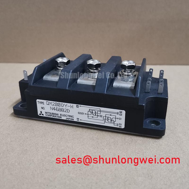
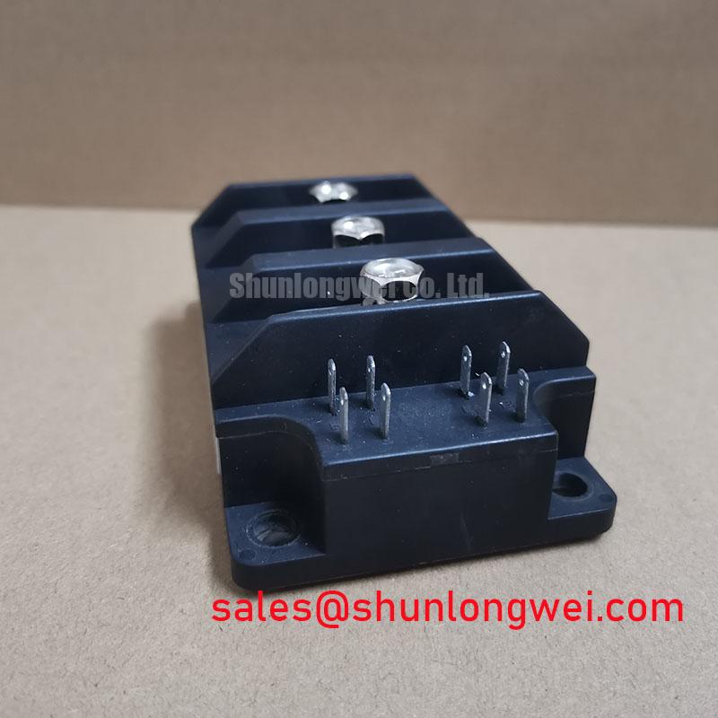
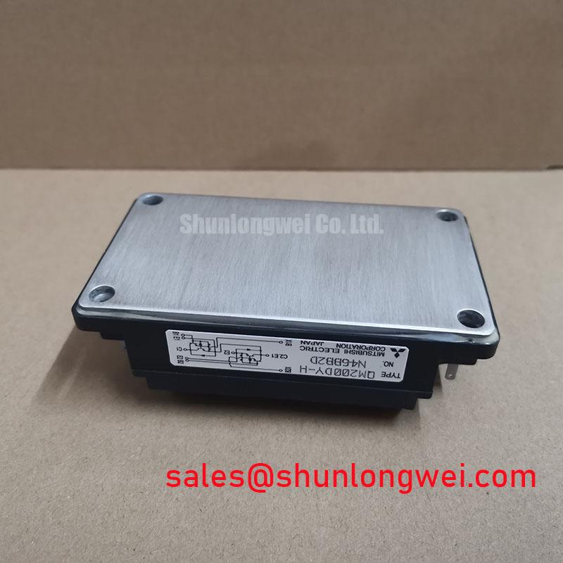
Before mounting the QM200DY-H, clean the heatsink surface, inspect the module baseplate for contamination or visible distortion, and confirm that the contact area is flat enough for the approved assembly method. The isolated Darlington package depends on the complete mechanical and thermal interface designed by the equipment manufacturer. A thin, continuous thermal interface layer is generally preferred as a Design Consideration, but the material type, application method, thickness, and mounting procedure should follow the original service documentation.
Excess compound can create cleanup problems and may reduce assembly consistency, while insufficient coverage can leave air-filled regions between the baseplate and heatsink. Apply the selected thermal interface material uniformly across the approved contact zone and avoid trapping debris. If a pre-applied pad or phase-change material is specified by the equipment builder, do not replace it with grease without confirming compatibility, compression behaviour, electrical insulation requirements, and service temperature.
Mounting screws should be tightened progressively in a cross pattern so that the baseplate seats evenly rather than being pulled down at one corner. The correct torque is an Official Assembly Specification only when stated in the relevant module or equipment manual. Otherwise, the maintenance team should treat the fastener value as a Design Consideration determined by screw size, thread condition, heatsink construction, and the manufacturer’s procedure.
Maintenance Note: isolate power and allow the DC link to discharge before touching the module, then periodically check contact temperature, fan airflow, terminal tightness, and thermal-interface condition.
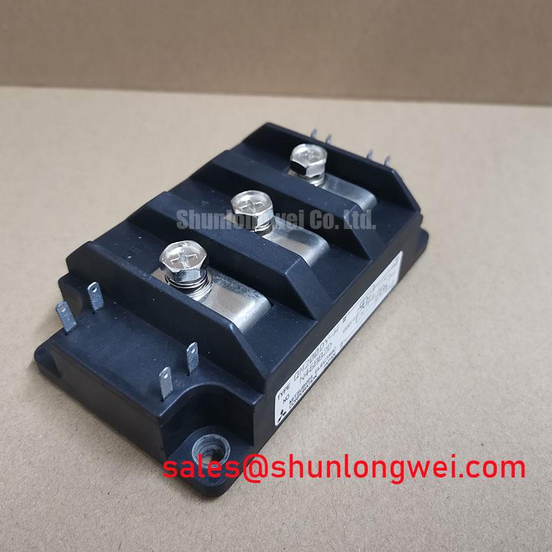
After installation, inspect the power terminals for even contact, confirm that busbars are not applying mechanical stress to the module, and check that control wiring cannot rub against the heatsink or high-voltage conductors. Perform a low-energy continuity and isolation review before applying the full DC link. During first energisation, monitor base-drive signals, collector-emitter behaviour, case temperature, fault feedback, and abnormal acoustic or electrical noise.
If thermal performance is poorer than the previous service record, compare the heatsink temperature profile, airflow path, interface coverage, mounting sequence, and load waveform. Do not treat a warm case as proof of internal failure without electrical and mechanical checks. A controlled comparison against the original installation record is the most reliable way to distinguish degraded cooling from altered switching conditions.