Shunlongwei Co. ltd.
IGBT Module / LCD Display Distributor
Customer Service
+86-755-8273 2562
IGBT Module / LCD Display Distributor
Intel CEO Pat Gelsinger showcased the world’s first Chiplet processor based on the UCIe connection at the Innovation 2023 conference. This chip integrates Intel UCIe IP chips manufactured on Intel’s 3rd-generation process node and Synopsys UCIe IP chips manufactured on TSMC’s N3E process node. The two Chiplets communicate through Intel’s EMIB interface.
The Universal Chiplet Interconnect Express (UCIe) interface has garnered support from numerous industry giants, including Intel, AMD, Arm, Nvidia, TSMC, Samsung, and 120 other companies. This interconnect design aims to standardize chip-to-chip interconnects between Chiplets through open-source design, reducing costs and fostering a more widely validated Chiplet ecosystem.

Current multi-Chiplet packaging relies on proprietary interfaces and protocols for communication, making it challenging to adopt third-party Chiplets widely. UCIe’s goal is to create an ecosystem with standardized interfaces, allowing chip manufacturers to easily select Chiplets from other designers and incorporate them into new designs with minimal design and validation effort.
The UCIe Alliance was established in 2022 and has gained extensive support from the chip manufacturing industry. The alliance has successively released UCIe 1.0 and 1.1 specifications. It has set ambitious performance and area targets, dividing the target market into two broad ranges using standard 2D packaging technology and more advanced 2.5D technology (EMIB, CoWoS, etc.). Advanced packaging options offer higher bandwidth and density.
Intel’s Chiplet-based processors, such as Sapphire Rapids and the newly announced Meteor Lake, currently use proprietary interfaces and protocols for Chiplet communication. However, Intel has announced its plans to use the UCIe interface after its next-generation consumer processor, Arrow Lake. AMD and Nvidia are also working on their plans but have not yet demonstrated available silicon chips.
As a long-standing leader in the semiconductor industry, renowned for its CPUs, Intel’s progress in processors is particularly noteworthy. During this conference, Intel presented a comprehensive showcase, marking the full-scale entry of Intel’s PC chips into the era of AI.
Gelsinger stated, “Artificial intelligence will fundamentally change, reshape, and reconstruct the PC experience, unleashing individual productivity and creativity through the power of cloud and PC collaboration. For this, Intel is ushering in a new era of AI computers.” The Intel Core Ultra processor, codenamed Meteor Lake, is a significant step towards achieving these goals.
In Intel’s view, Core Ultra represents a turning point in Intel’s client processor roadmap, as it is the first client Chiplet design supported by Foveros packaging technology (Intel’s 3D packaging technology) and utilizes EUV lithography. From a design perspective, the chip includes four parts: computing tile, graphics tile, SoC tile, and I/O tile. The computing tile is based on Intel’s 4th-generation process, the graphics tile is based on TSMC’s 5nm process, and the SoC tile uses TSMC’s 6nm process, embodying the spirit of Chiplet technology. It’s worth noting that this chip’s SoC tile also integrates Intel’s first NPU.
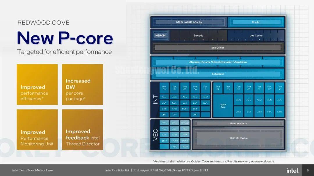
Regarding specific chip design details, it was revealed that the computing tile of the chip includes a pair of new cores, one named Redwood Cove P-core and a new E-core named Crestmont. The new P-core is a direct successor to Intel’s 12th-generation core (Raptor Lake) processors’ previous Golden Cove core, and the new Redwood Cove core brings significant IPC improvements to Intel’s chip processors.
As for the E-core, it was reported that it maintains AI acceleration based on CPU through Vector Neural Network Instructions (VNNI). Similar to the P-core, the E-core also benefits from enhanced Thread Director feedback, providing better granularity control and optimization.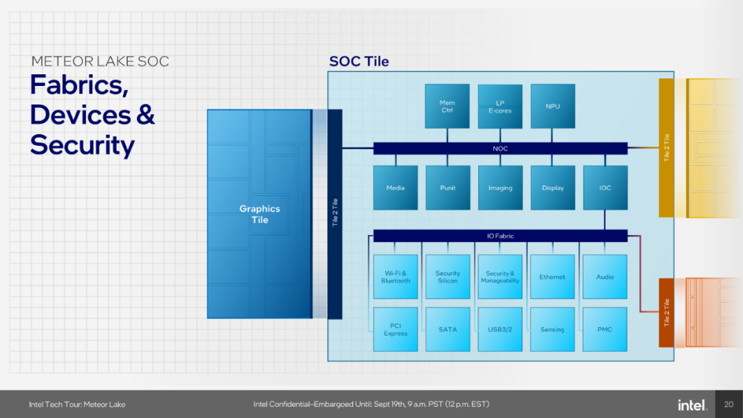
Regarding SoC tiles, it was explained that Intel has eliminated the old limitations of mesh routing by implementing on-chip networks (NOC) on the silicon. This is not only to make data channels faster but also to achieve more intelligent and energy-efficient memory access. After leveraging EMIB and 2D scaling, the data paths are significantly shorter, reducing power consumption. However, the shorter wires also help reduce overall latency loss.
As mentioned earlier, this SoC tile also features a fully functional Neural Processing Unit (NPU), which is Intel’s first NPU for client processors. Thanks to this module, Intel can directly introduce AI capabilities into client chips, and because it is compatible with standardized programming interfaces like OpenVINO, it brings convenience during development. This NPU comprises two neural computing engines that can collaborate on single tasks or run independently. These neural computing engines mainly consist of two components: the inference pipeline and SHAVE DSP.