


Content last revised on June 29, 2026
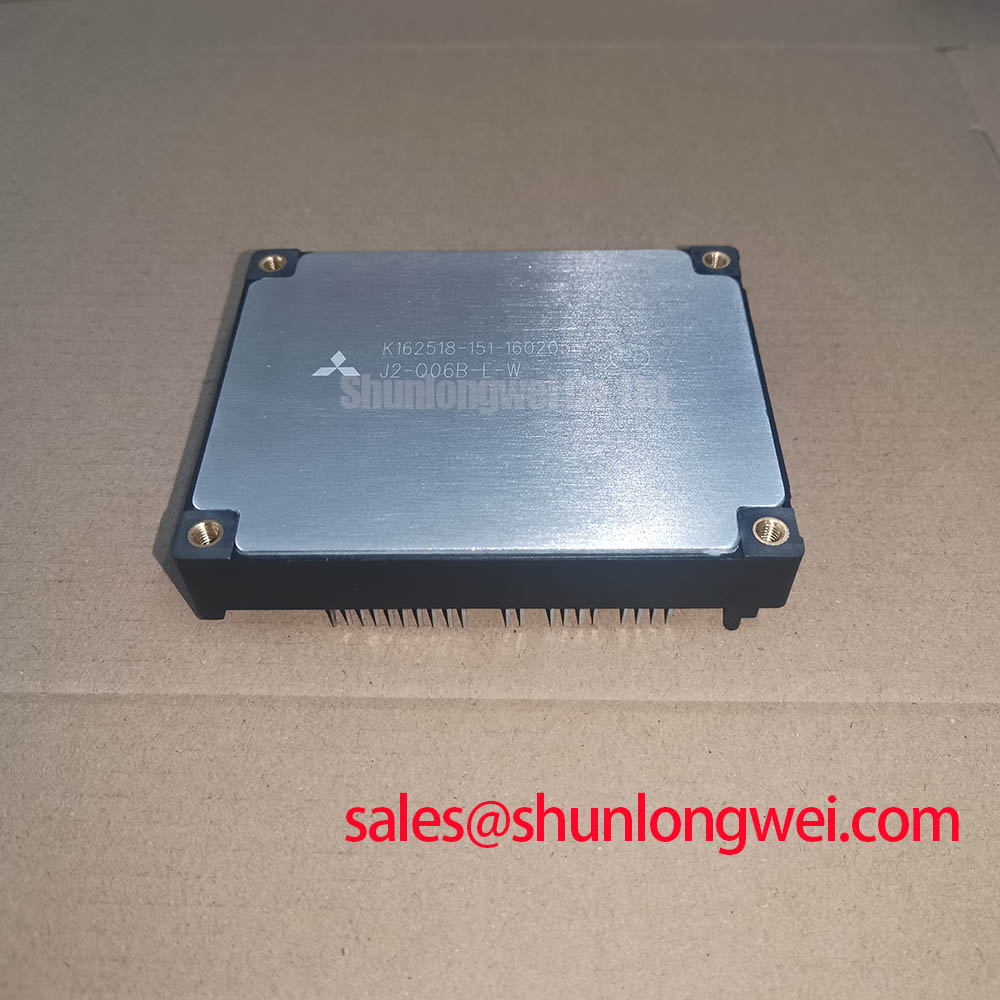
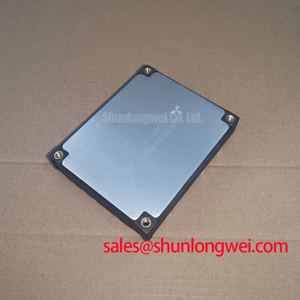
J2-Q06B-E-W DIPIPM™: Technical Review of a 600V/6A Integrated Power Module for Compact Motor Drives
Introduction and Key Highlights
Streamlining Low-Power Inverter Design
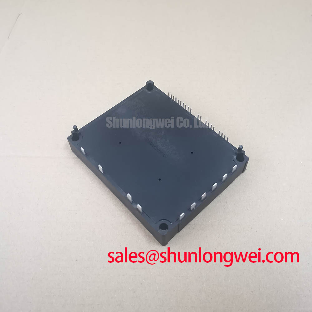
The Mitsubishi J2-Q06B-E-W is a DIPIPM™ engineered to accelerate the design of reliable and compact three-phase inverter stages by integrating power devices, gate drivers, and protection circuits into a single module. With core specifications of 600V | 6A | Integrated HVIC/LVIC, this Intelligent Power Module (IPM) offers the key benefits of a drastically reduced component count and a significantly accelerated design cycle. It directly addresses the challenge of developing small motor drives by providing a pre-optimized and tested power stage solution. For space-constrained appliance motor drives up to approximately 0.75kW, the J2-Q06B-E-W is a definitive choice for simplifying system design and enhancing reliability.
Key Parameter Overview
Decoding the Electrical Characteristics for System Integration
The electrical characteristics of the J2-Q06B-E-W are tailored for efficiency and reliability in low-power applications. The parameters outlined below are critical for system-level design, particularly for thermal management and interfacing with control logic. The highlighted values represent the primary operational limits and foundational specifications for any design project.
| Highlighted Key Specifications | ||
| Parameter | Symbol | Rating |
| Collector-Emitter Voltage | VCES | 600V |
| Collector Current (DC) | IC | 6A |
| Control Supply Voltage | VCC | 20V |
| Bootstrap Diode Forward Voltage | VF | Typ. 2.6V |
| Additional Performance Characteristics (Tj=25°C unless noted) | ||
| Parameter | Conditions | Value |
| Collector-Emitter Saturation Voltage (VCE(sat)) | IC = 6A | Typ. 1.7V |
| Control Supply UV Protection Trip Level | VCCH/L(U)T | 11.3V - 13.5V |
| Thermal Resistance (Junction-to-Case) | Rth(j-c) | Typ. 4.9°C/W per IGBT |
The low VCE(sat) is a critical parameter for efficiency. Think of it like a water valve: a lower VCE(sat) value means the "valve" opens wider when the IGBT is on, presenting less resistance to the current (water flow). This directly translates to lower conduction losses and less heat generation, simplifying thermal design.
Application Scenarios & Value
System-Level Benefits in Appliance and Light Industrial Automation
The J2-Q06B-E-W is engineered to deliver significant value in applications where board space, reliability, and development speed are critical design constraints. Its primary role is as the core of a three-phase inverter for low-power motor control.
Consider the design of a motor controller for a high-efficiency, variable-speed Brushless DC (BLDC) motor in a modern washing machine. A key engineering challenge is to create a compact control board that fits within a constrained chassis while ensuring high reliability over a 10+ year appliance lifetime. Using a discrete solution with separate IGBTs, gate drivers, and protection circuits would consume significant PCB area and introduce complex layout challenges to manage parasitic inductance. The J2-Q06B-E-W directly solves this by consolidating these functions. Its integrated nature, including the internal bootstrap circuit components, reduces the overall footprint by over 50% in many cases. Furthermore, the built-in under-voltage (UV) lockout ensures the module shuts down safely during power grid sags, preventing erratic behavior and protecting the motor windings.
This level of integration makes the J2-Q06B-E-W ideal for:
- Home Appliances (Washing Machines, Air Conditioners, Fans)
- Light Industrial Automation (Small Conveyor Belts, Pumps)
- General-Purpose Low-Power Inverters
While the J2-Q06B-E-W is optimized for these lower-power systems, for designs requiring higher current and voltage handling, such as industrial servo drives, a related module like the 6MBP25VAA120-50 provides a 1200V, 25A rating in an intelligent power module format.
Technical Deep Dive
A Closer Look at the Integrated HVIC and Protection Architecture
The core innovation within the J2-Q06B-E-W lies in its highly integrated High-Voltage and Low-Voltage ICs (HVIC and LVIC). This architecture provides a level of optimization that is difficult to achieve with discrete components. In a traditional design, engineers must carefully lay out the path from the gate driver IC to the IGBT gates to minimize parasitic inductance, which can cause voltage overshoots and ringing. The IPM architecture of the J2-Q06B-E-W inherently solves this by co-locating the drivers and power switches within the same package, creating extremely short, optimized connections.
A crucial element of this integration is the built-in bootstrap diodes (BSD) and their associated current-limiting resistors. For the high-side IGBTs in a three-phase bridge, a floating power supply is required for the gate drivers. The bootstrap circuit is a common and cost-effective way to create this supply. However, designing it from scratch requires careful calculation and component selection (diode, resistor, capacitor) to ensure the gate voltage is stable across all operating frequencies and duty cycles. The J2-Q06B-E-W removes this design burden entirely. The integrated BSD is pre-matched to the gate driver's requirements, ensuring robust high-side switching without the risk of an undercharged bootstrap capacitor, a common failure mode in discrete designs. This allows the system designer to simply provide the main control power and PWM signals from a microcontroller (MCU), confident that the power stage is self-contained and robust.
Frequently Asked Questions (FAQ)
Engineering Questions on Implementation and Reliability
What is the primary benefit of the integrated bootstrap diodes (BSD) in the J2-Q06B-E-W?
The primary benefit is design simplification and enhanced reliability. It eliminates the need for external bootstrap components (diodes and resistors), saving board space and reducing the component count. This pre-optimized internal circuit ensures robust and reliable power for the high-side gate drivers under all specified operating conditions.
What are the key considerations when interfacing the J2-Q06B-E-W with a microcontroller (MCU)?
The key considerations are ensuring the logic levels are compatible (typically 3.3V or 5V), providing a clean control power supply (VCC) within the specified range, and implementing a dead-time between the high-side and low-side PWM signals of a single phase to prevent shoot-through. The module's input pins are typically high-impedance, making them easy to drive directly from standard MCU I/O ports.
How does the control supply under-voltage (UV) protection enhance system safety?
The UV protection continuously monitors the gate driver's supply voltage (VCC). If this voltage drops below a safe level, the gate drive logic is disabled, and a fault signal is typically asserted. This prevents the IGBTs from operating with insufficient gate voltage, which could lead to increased conduction losses, overheating, and eventual failure. It ensures a controlled shutdown during power sags, protecting both the module and the load.
What is the main advantage of an IPM over a discrete design?
The main advantage is drastically reduced design complexity and improved system reliability by integrating key components and optimizations.
The strategic adoption of the J2-Q06B-E-W allows engineering teams to de-risk the most challenging part of inverter design—the power stage. By leveraging a pre-validated, highly integrated module, companies can redirect resources from low-level power electronics tuning to higher-value software development and feature differentiation. This shift not only accelerates time-to-market for products like energy-efficient appliances and automated systems but also enhances final product reliability, ultimately strengthening a company's competitive position in a crowded marketplace.