




Content last revised on October 12, 2026
J2S-Q01A-D Operational Boundaries: Evaluating Symmetrical Busbar Geometry for High-Current Paths
- Confirm the cold-state terminal-to-terminal readings against the approved service reference before applying drive power.
- Check the module seating surface, thermal interface condition, and busbar alignment before tightening the power terminals.
- Verify control-drive polarity, driver isolation, and high-side supply continuity with the DC link fully discharged.
- Record the approved insulation tester setup before checking terminal-to-baseplate isolation.
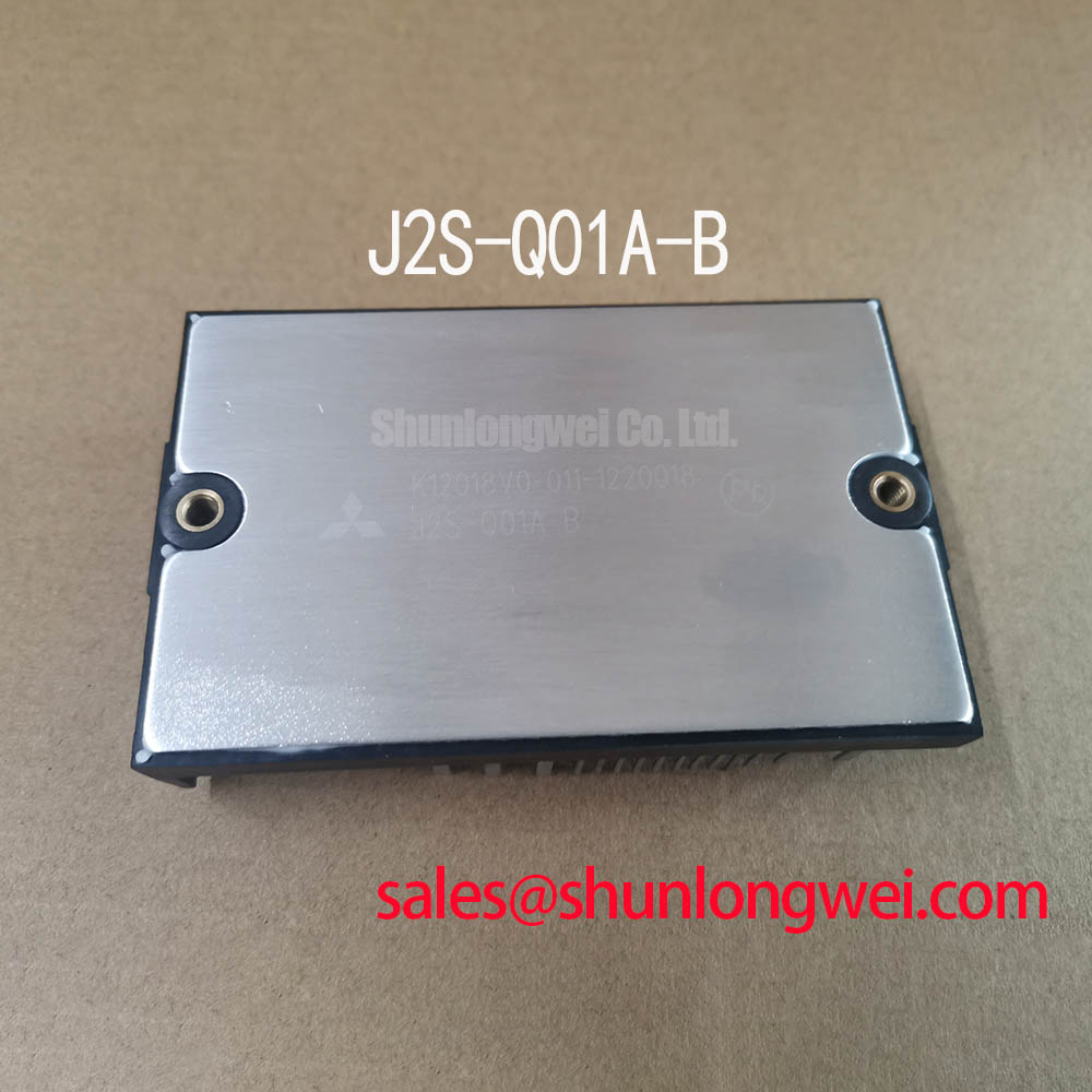
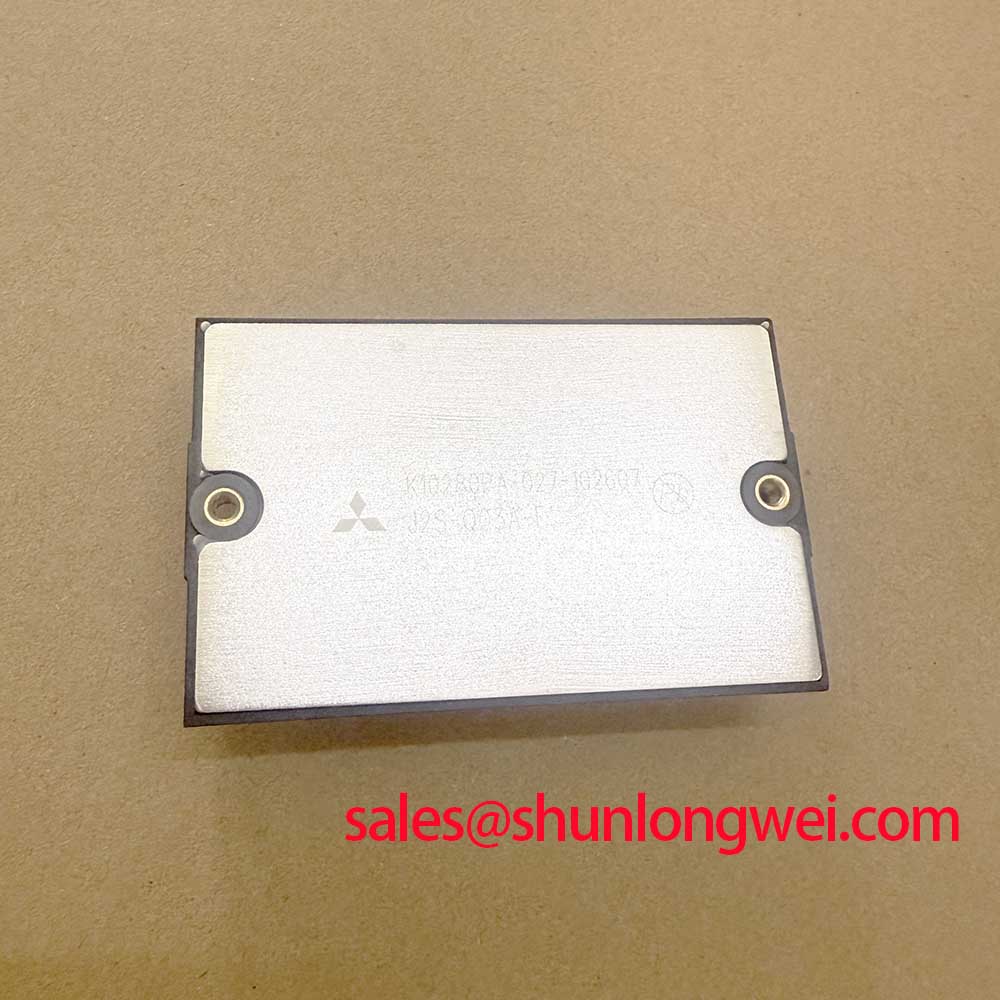
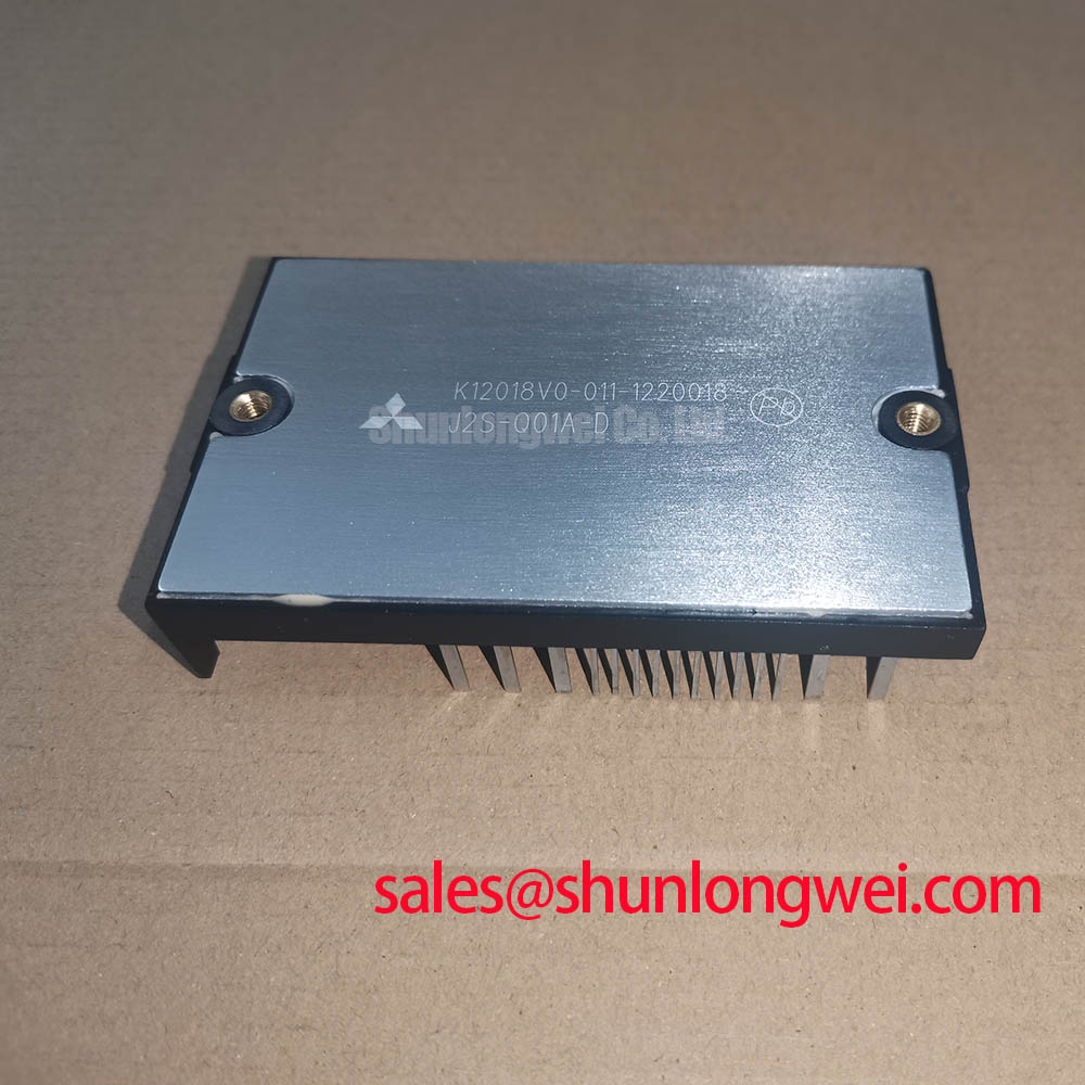
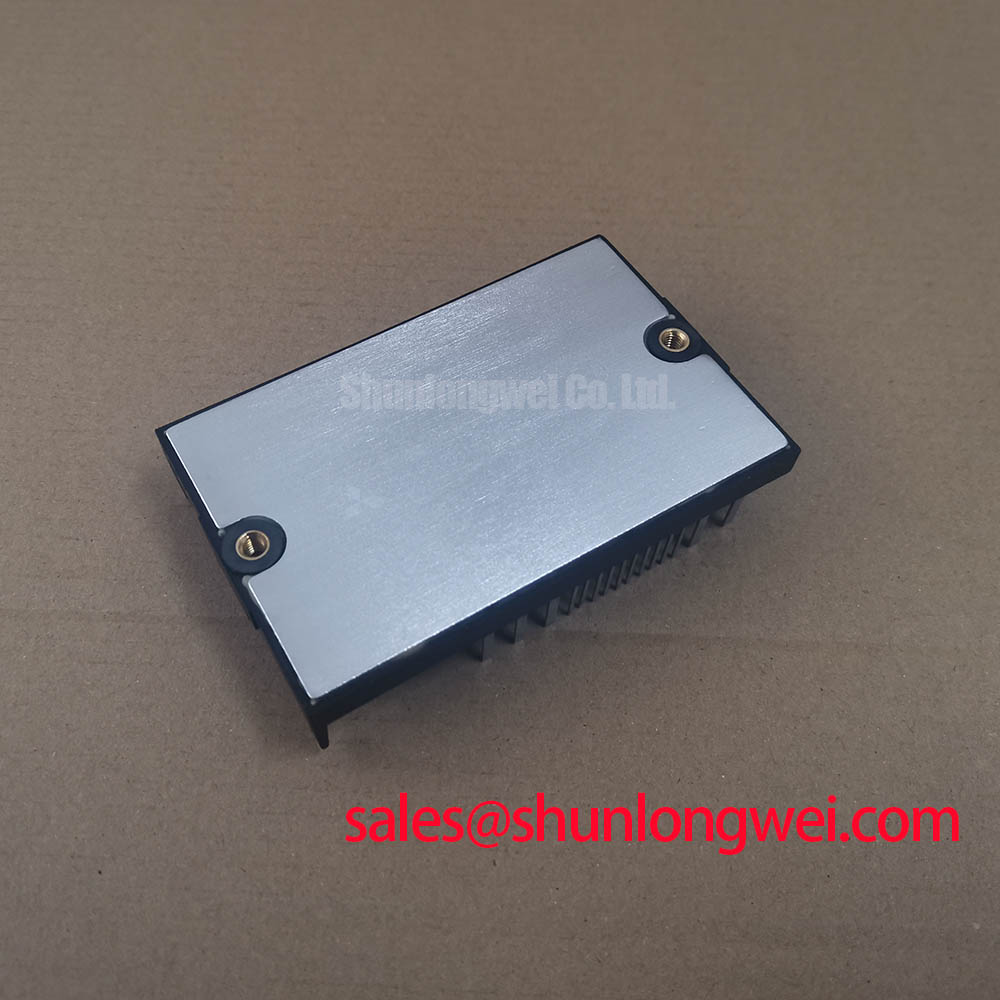
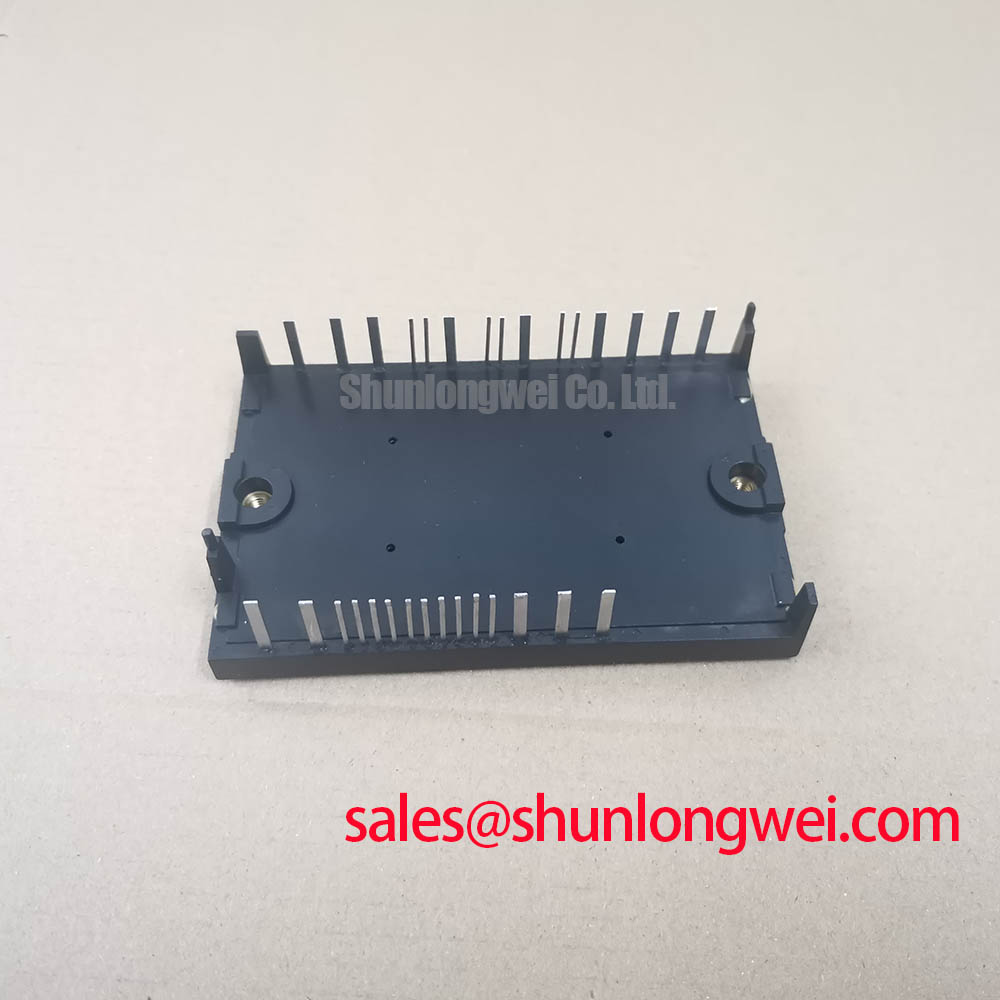
J2S-Q01A-D from Fuji Electric is identified as a power transistor module for industrial power conversion work. The available product information does not establish numerical voltage or current ratings. Generic descriptions such as “Standard Industrial Rating” and “Standard Operating Current” are not usable electrical specifications. Confirm the exact device ratings and terminal configuration from the manufacturer’s documentation or the approved equipment service reference before applying power.
| Parameter | Product information | Engineering use |
|---|---|---|
| Manufacturer | Fuji Electric | Confirm the original equipment bill of materials before replacement |
| Part number | J2S-Q01A-D | Use the complete suffix when matching service records and terminal layout |
| Product category | Power transistor module; confirm the exact transistor type | Evaluate as a power switching device within the original circuit topology |
| Voltage rating | Not established by the available product information | Verify the documented rating against the original DC bus and transient conditions |
| Current rating | Not established by the available product information | Assess the documented rating and its conditions together with cooling and duty cycle |
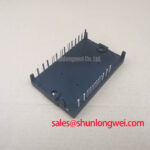
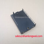
| Housing | Power Transistor Module | Inspect mounting flatness, terminal clearance, and heat-transfer path |
| Isolation reference | Confirm the permitted test voltage and acceptance criteria in the approved documentation | Use an insulation tester for terminal-to-baseplate verification only when the documented procedure permits it |
Fuji Electric’s power semiconductor and IPM module information provides useful background for engineers comparing module-level construction and application requirements. For a replacement assessment, the correct procedure is to compare the physical terminal arrangement, the control-drive interface, the baseplate mounting pattern, and the electrical stress recorded in the original machine. A familiar package appearance is not sufficient evidence of circuit compatibility.
The gate-drive examples below apply to gate-controlled switching stages and should not be taken as confirmation of the J2S-Q01A-D’s internal structure. If the approved documentation identifies a bipolar or Darlington transistor, use its specified base-drive requirements instead; gate-charge and bootstrap guidance cannot be transferred directly to that device.
Symmetrical busbar geometry is the first practical control point when several current paths share a power transistor module or when a traction inverter uses parallel conduction paths. Keep the positive and return conductors physically balanced around the intended current loop, and avoid allowing one branch to become noticeably longer, narrower, or more inductive than its counterpart. The purpose is not cosmetic symmetry; it is to prevent unequal voltage drop and unequal switching-loop impedance from forcing one path to carry a disproportionate transient current.
A positive temperature coefficient of VCE(sat), where documented for the device at the relevant operating point, can support steady-state current sharing because a warmer conducting path tends to develop a higher conduction voltage. This behavior must not be assumed for every transistor type or current range. This effect should be treated as a stabilizing tendency rather than a substitute for matched wiring. Dynamic sharing occurs during the much shorter switching interval, when control-loop inductance, emitter or return-path impedance, driver timing, and busbar placement can dominate the result. Designers should therefore route matched control-drive and return connections together and keep their physical relationship consistent from the driver board to the module terminals.
For an electric forklift or warehouse vehicle traction controller, inspect the busbar transition from the DC-link capacitor to the switching stage as a complete current loop. A sharp bend, a loose laminated-busbar joint, or an unplanned branch connection can create local voltage overshoot even when the measured battery voltage appears normal. During service testing, compare the voltage at the module terminals rather than relying only on a remote DC-link measurement. An oscilloscope with suitable differential probes can reveal whether the apparent imbalance is associated with busbar inductance, drive timing, or a mechanical connection.
Mounting alignment also affects electrical repeatability. The module baseplate should sit evenly on the prepared heat-transfer surface, while the power terminals remain free from mechanical loading caused by a misaligned busbar. Do not use terminal screws to pull a distorted conductor into position. First correct the conductor alignment, then tighten the connection according to the equipment manufacturer’s documented procedure. The required thermal interface material and mounting force are system and assembly requirements; they should not be inferred from the product category alone.
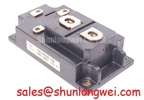
When evaluating a possible alternative in the same general power-conversion family, engineers may place 1DI400A-140 beside the original part in a comparison worksheet. This is a neutral cross-reference exercise, not an automatic substitution. Terminal geometry, electrical ratings, control-drive characteristics, thermal impedance, and protection coordination all require independent review before a design change.
A useful field measurement is to capture the control-drive waveform at the module pins while also observing the collector-to-emitter switching node. For a gate-controlled device, this includes the gate-to-emitter voltage; a bipolar device also requires assessment of base-drive current. Compare the rising and falling transitions of each channel under the same load condition. Unequal drive amplitude, different turn-on delay, or a ringing tail may indicate a layout or driver-path mismatch. Correct the physical path and repeat the measurement before changing protection thresholds or increasing the drive.
J2S-Q01A-D Operational Boundaries: Evaluating Switching-Current Ringing and Diode Recovery
Where the switching circuit uses an antiparallel freewheeling diode, its reverse-recovery behavior has a direct influence on turn-on stress because its reverse-recovery current can overlap the rising collector current of the transistor. The relevant observation is the shape and duration of the recovery pulse, not only its peak value. A sharp recovery characteristic can produce a high di/dt, which combines with stray inductance to create voltage ringing, conducted noise, and additional semiconductor stress.
Begin the switching review by placing the current probe and voltage probe close to the module terminals. A remote probe location can hide the local recovery event or show a waveform that is dominated by the busbar rather than by the device. Compare the waveform with the original service unit or with a known-good assembly operated under the same load and DC-link conditions. If the ringing follows the physical arrangement rather than the replacement device, inspect the commutation loop, capacitor placement, and terminal clamping before changing the drive network.
In a gate-controlled switching stage, the turn-on gate resistance influences the speed at which the transistor accepts current. Increasing the resistance can be considered as a damping adjustment when the measured recovery event produces excessive ringing, but it also changes switching loss and thermal loading. Any value selected for a trial should be treated as a starting point for bench tuning, followed by temperature measurement and switching-waveform verification. The final setting is determined by the complete converter, not by the module label alone.
RC snubber selection follows the same principle. The snubber must absorb the targeted high-frequency energy without creating unnecessary continuous loss. Place the network close to the switching loop it is intended to control, and evaluate its voltage rating, pulse capability, layout inductance, and temperature rise under the actual switching pattern. A snubber connected far from the module may have limited effect because the unwanted inductance remains between the device and the damping network.
High-side drive power integrity deserves separate attention. In a gate-controlled stage using a bootstrap supply, a bootstrap capacitor must supply the gate charge demanded during the high-side conduction interval while also covering driver quiescent current, leakage, refresh timing, and voltage ripple. In practical terms, select the capacitor by accounting for total charge demand and then verify the high-side supply waveform at the driver pins during the longest intended on-time. The driver manufacturer’s limits, the selected switching frequency, and the duty-cycle range determine whether the bootstrap method is appropriate.
Do not connect a replacement module to a high-side driver until the driver reference node, supply return, and control-terminal polarity have been traced from the schematic and the physical board. A continuity check with the control supply removed can confirm the intended path, but it cannot prove correct dynamic operation. After static checks, use a current-limited test condition and observe control-drive voltage, switching-node voltage, and driver supply behavior together.
For equipment using a rectifier stage ahead of an inverter, review the rectifier, DC-link capacitor, precharge circuit, switching bridge, and braking path as separate functional blocks, then verify how a fault in one block can impose stress on the next. A related power module such as 6DI75A-050 does not define the ratings or protection settings of the J2S-Q01A-D stage; its device type and circuit role require separate verification.
💡 Bench Tip: Keep the device in an ESD-controlled work area and record cold-state diode and terminal readings before attaching the driver, then compare those readings with the known-good assembly rather than relying on a single meter result.
J2S-Q01A-D Circuit Protection & Reliability: Verifying Terminal-to-Baseplate Insulation
Terminal-to-baseplate isolation should be checked with the power circuit completely disconnected, the DC link discharged, and all control and sensing connections isolated from the test voltage. Confirm the permitted test voltage, test duration, terminal grouping, and acceptance criteria in the manufacturer’s documentation or approved equipment procedure before testing. Apply the insulation tester between the documented terminal group and the metal baseplate only when that procedure permits the connection. Sensitive driver boards, current sensors, capacitors, and communication circuits must not remain attached to the test point. Discharge the tested assembly safely after the test.
The test environment affects repeatability. Dust, conductive residue, moisture, and flux contamination can create a surface leakage path across the mounting region even when the internal isolation system is intact. Clean the accessible mounting surface using an approved process, allow it to dry, and inspect the area around terminal barriers and fasteners. Creepage distance is measured along the surface; clearance is the direct air path. Both matter when airborne dust can collect around a power module, particularly inside a vehicle controller or warehouse charging cabinet.
A failed or unstable insulation reading should lead to a controlled separation of possible paths. First remove external harnesses and confirm that the tester itself is functioning correctly and connected as specified. Next inspect the baseplate, mounting hardware, terminal supports, and nearby contamination. If the reading changes when the module is isolated from the assembly, the external circuit may be contributing to the leakage. If the behavior remains associated with the module, quarantine the component for engineering assessment instead of returning it immediately to service.
Short-circuit protection requires coordination between the circuit’s fault-detection method, the driver’s turn-off response, the DC-link protection, and the upstream semiconductor fuse. Where desaturation or collector-emitter voltage monitoring and soft turn-off are used, a soft turn-off strategy can reduce the voltage excursion created when a fault current is interrupted, but the response must be checked with the actual driver propagation delay, control-drive loop, and fault-current path. The protection threshold and blanking interval are system parameters and should be calibrated using the approved driver documentation and controlled fault testing.
Fast semiconductor fuses are selected by comparing their clearing behavior with the converter’s short-circuit energy and the module’s permitted fault stress. The fuse’s I2t value should be coordinated with the protection study rather than copied from a different voltage class or fuse family. Fuse coordination alone does not guarantee transistor protection. A fuse that interrupts slowly may allow damaging energy to reach the module, while an incorrectly selected fast fuse can create nuisance operation during legitimate traction-current peaks. The equipment protection designer must evaluate the complete battery, contactor, precharge, DC-link, and inverter path.
Thermal installation remains part of reliability verification. The baseplate and heatsink must be clean, flat, and free of burrs before applying the specified thermal interface material. Excess material can increase the thermal path, while an incomplete spread can leave localized hot regions. Tighten the mounting hardware in the documented sequence so the baseplate is not warped during assembly. ⚠️ Field Alert: Never insert or remove the control-drive, control, or power connector while the DC link or driver supply is energized.
When the module is evaluated for a low-voltage traction controller, repeated vehicle operating cycles can impose thermal transitions through the power stage. The appropriate review focuses on junction-temperature swing, heatsink temperature, current profile, braking duty, and enclosure airflow measured on the actual vehicle platform. Do not convert a generic operating-current label directly into a lifetime prediction. Record the thermal waveform and switching duty first, then compare it with the manufacturer’s qualified operating limits and the original controller’s protection strategy.
For service teams studying commutation behavior in household or industrial power converters, the reference article Resonant Topologies in Home Appliances offers a useful topology-level comparison. The operating principle may assist waveform interpretation, but it does not replace the J2S-Q01A-D terminal map, isolation test, mechanical installation procedure, or the original equipment protection documentation.