Shunlongwei Co. ltd.
IGBT Module / LCD Display Distributor
Customer Service
+86-755-8273 2562
IGBT Module / LCD Display Distributor
“From power supplies and motor drives to charging stations and countless other applications, switching power semiconductors such as silicon (Si), silicon carbide (SiC) and gallium nitride (GaN) MOSFETs and insulated gate bipolar transistors (IGBTs) enable high efficiency The key to power system design. However, for maximum performance from a power supply, proper gate drivers are required.
“
By Bill Schweber
From power supplies and motor drives to charging stations and countless other applications, switching power semiconductors such as silicon (Si), silicon carbide (SiC) and gallium nitride (GaN) MOSFETs and insulated gate bipolar transistors (IGBTs) enable high efficiency The key to power system design. However, for maximum performance from a power supply, proper gate drivers are required.
As the name implies, a gate driver acts to drive the gate of a power supply device into or out of conduction mode quickly and neatly. To do this, the driver needs to be able to source/sink enough current regardless of internal components and stray (parasitic) capacitance, inductance, and other issues at the load (gate) side. Therefore, providing gate drivers with the right dimensions and with the right key attributes is critical to unlocking the maximum potential and efficiency of power supply devices. However, to get the most out of the gate driver, designers must pay special attention to the driver’s DC power supply, which is independent of the DC rails of the power supply unit. This power supply is similar to a conventional power supply with some important differences. It can be a unipolar power supply, but in many cases it is an asymmetrical bipolar power supply, along with other functional and structural differences. In addition, designers must pay attention to form factor, including board footprint and low profile requirements, as well as compatibility with the intended assembly and manufacturing process of the design.
This article will focus on gate driver power supplies using surface mount device (SMD) DC/DC power supplies in Murata Power Solutions’ MGJ2 series of 2 W gate drive DC/DC converters as examples.
Start with switching devices
To understand the role and required properties of a gate driver DC/DC converter, one needs to start with switching devices. In a MOSFET used as a switching device, the gate-source path can be used to control the off or on state of the device (similar to IGBTs). When the gate-source voltage is less than the threshold voltage (VGS
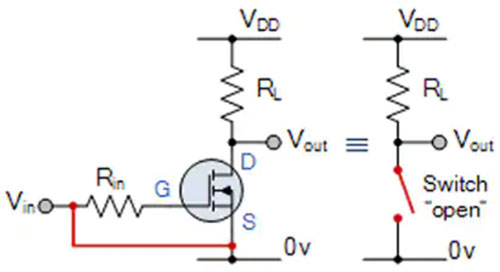
Figure 1: In cutoff mode, the MOSFET drain-source path looks like an open switch. (Image credit: Quora)
Conversely, when the gate-source voltage is much greater than the threshold voltage (VGS > VTH), the MOSFET is in the saturation region with maximum leakage current flowing (ID = VDD /RL) and the MOSFET looks like a “closed switch” (Figure 2). For an ideal MOSFET, the drain-source voltage is zero (VDS = 0 V), but in practice VDS is typically 0.2 due to the internal on-resistance RDS(on) (typically below 0.1 Ω, and possibly as low as tens of mΩ) V or so.
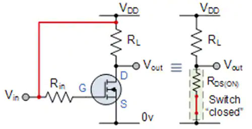
Figure 2: In saturation mode, the MOSFET drain-source path looks like a low-resistance switch. (Image credit: Quora)
While the schematic makes it appear that the voltage applied to the gate causes the MOSFET to turn on and off, this view is not comprehensive. This voltage drives current into the MOSFET until there is enough accumulated charge to turn it on. Depending on the size (current rating) and type of the switch driver, the amount of current required to quickly go to full conduction can be in the range of a few mA to a few A.
The function of the gate driver is to quickly and cleanly drive enough current into the gate to turn the MOSFET on, and to pull that current in reverse to turn the MOSFET off. More formally, the gate needs to be driven by a low-impedance power supply that can source and sink enough current to allow fast insertion and extraction of controlled charges.
Sourcing and sinking this current would be relatively simple if the MOSFET gate looked like a purely resistive load. However, not only do MOSFETs have internal capacitive and inductive parasitics, but there are also parasitic effects from interconnecting devices between the driver and power supply unit (Figure 3).
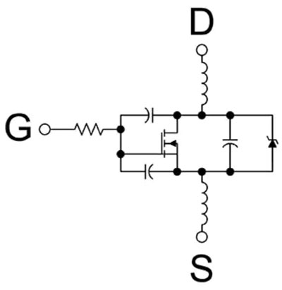
Figure 3: This MOSFET model shows parasitic capacitance and inductance that affect driver performance. (Image credit: Texas Instruments)
The gate drive signal then oscillates as it approaches the threshold voltage, causing the device to turn on and off one or more times on a fully on or off trajectory; this is somewhat analogous to the “switch bounce” of a mechanical switch phenomenon (Figure 4).
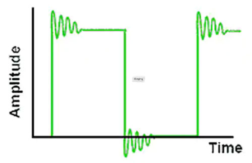
Figure 4: Ringing at the driver output due to parasitics in the MOSFET load, resulting in ringing and false triggering similar to mechanical switch bounce. (Image credit: Learn About Electronics)
This phenomenon has a wide range of effects: as small as in inconsequential applications like switching lights on and off, which can cause subtle effects that no one will notice or are only somewhat annoying; as large as in power supplies, motor drives and similar subsystems , may cause damage to widely used pulse width modulation (PWM) fast switching circuits. In standard half-bridge and full-bridge topologies, since the load is placed between the upper and lower pair of MOSFETs, if both MOSFETs on the same side of the bridge are turned on at the same time, even for a moment, it will cause a short circuit, or even permanently. sexual damage. This phenomenon is called “breakdown” (Figure 5).
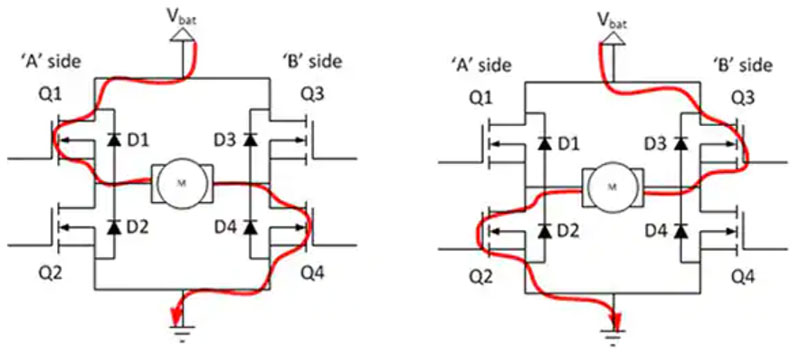
Figure 5: Compared to normal MOSFET turn-on (Q1 and Q4 (left) or Q2 and Q3 (right)), if due to driver issues or other reasons, both Q1 and Q2 or Q3 and Q4 of the bridge are turned on at the same time , an unacceptable and potentially damaging short circuit occurs between the power rail and ground, also known as “shoot-through”. (Image credit: Quora)
Gate Drive Details
In order to drive current into the gate, the positive voltage of the rail should be high enough to ensure that the power switch is fully saturated/boosted, but should not exceed the absolute maximum voltage of its gate. Although this voltage value depends on the specific device type and model, IGBTs and standard MOSFETs are typically fully turned on with a drive voltage of 15 V, while typical SiC MOSFETs may require drive voltages approaching 20 V to fully turn on.
The situation with negative gate drive voltages is a little more complicated. In principle, for the off state, it is sufficient to maintain 0 V on the gate. However, with a negative voltage (usually between -5 V and -10 V), fast switching controlled by the gate resistor can be achieved. A properly negative drive voltage ensures that the gate-emitter turn-off voltage is always practically zero or lower.
This is critical because any emitter inductance (L) between the switch and the driver reference (at point “x” in Figure 6) will cause a reverse gate-emitter voltage when the switch turns off. While this inductance may be small, even a tiny 5 nH Inductor (a few millimeters of wire connection) can produce 5 V with a di/dt slew rate of 1000 A/μs.
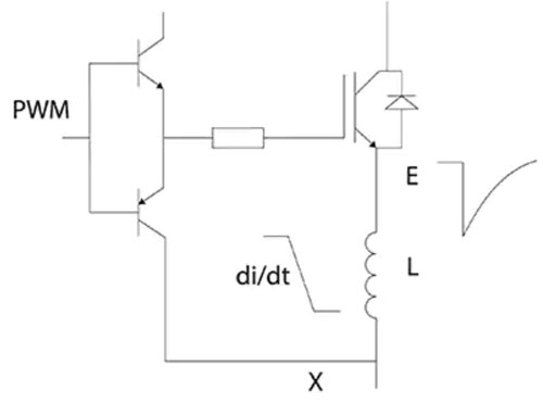
Figure 6: Due to layout considerations, even a small emitter inductance at point “x” between the switch and the driver reference will induce a reverse gate-emitter voltage when the switch is turned off, causing a On/off “jitter”. (Image credit: Murata Power Solutions)
The negative gate drive voltage also helps overcome the collector/drain-gate Miller effect capacitance Cm, which injects current into the gate drive circuit during device turn-off. When the device is turned off, the collector-gate voltage rises and a current of value Cm × dVce/dt flows through the Miller capacitor, into the gate-to-emitter/source capacitor Cge, and through the gate resistor to the driver circuit . The voltage Vge developed on the gate may be sufficient to turn the device on again, causing possible breakdown and damage (Figure 7).
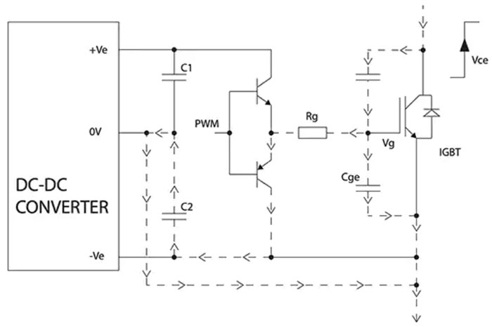
Figure 7: Using a negative gate drive voltage can overcome the disadvantages due to the presence of Miller effect capacitance in a MOSFET or IGBT. (Image credit: Murata Power Solutions)
However, with negative gate drive voltages, this effect is minimized. For this reason, an effective driver design requires both positive and negative voltage rails for gate drive functionality. However, unlike most bipolar DC/DC converters with symmetrical outputs such as +5 V and -5 V, the gate driver’s power rails are usually asymmetric, with more positive voltages than negative ones.
Determine the power rating of the converter
One of the key factors is how much current the gate drive converter must deliver, and thus how much power rating. The basic calculation process is very simple. During each switching cycle, the gate must be charged and discharged through the gate resistor Rg. The data sheet for this device provides a plot of gate charge Qg, where Qg is the amount of charge that needs to be injected into the gate electrode to turn on (drive) the MOSFET at a particular gate voltage. Use the following formula to find the power that must be provided by the DC/DC converter:
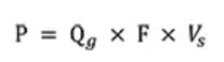
where Qg is the gate charge corresponding to the selected gate voltage swing (positive to negative, value Vs, frequency F). This power is dissipated in the device’s internal gate resistor (Rint) and the external series resistor, Rg. Most gate drivers require less than one to two watts of power.
Another consideration is the peak current (Ipk) required to charge and discharge the gate. This is a function of Vs, Rint and Rg. It is calculated using the following formula:
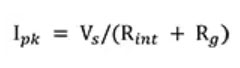
In many cases, this peak current is beyond what the DC/DC converter can provide. Instead of using a larger, more expensive power supply (operating at a low duty cycle), most designs use bulk capacitors on the driver supply rails to supply the current, which are carried out by the converter during the low current cycle portion Charge.
These bulk capacitors can be sized through basic calculations. But just as importantly, they must have low equivalent series resistance (ESR) and inductance (ESL) so as not to interfere with the instantaneous currents they carry.
Other Gate Drive Converter Considerations
Gate driver DC/DC converters also face other unique problems. These include:
• Regulation: When the DC/DC converter is not switching, the load on the device is close to zero. However, most conventional converters require an extremely small load at all times; otherwise, their output voltage can increase dramatically, possibly even reaching gate breakdown levels.
Here’s what happens: This high voltage is stored on the bulk capacitor, causing gate overvoltage when the device starts to switch, until the converter level drops under normal load. Therefore a DC/DC converter with clamped output voltage or very low minimum load requirements should be used.
• Startup and Shutdown: It is important that the IGBTs and MOSFETs are not actively driven by the PWM control signal until the voltage rail of the driver circuit has reached a specified value. However, when the gate drive converter is powered up and down, there may be a transient condition that can drive the device on even when the PWM signal is inactive, causing breakdown and damage to the device. Therefore, the DC/DC converter output should remain stable at power up and power down, with a monotonic rise and fall (Figure 8).
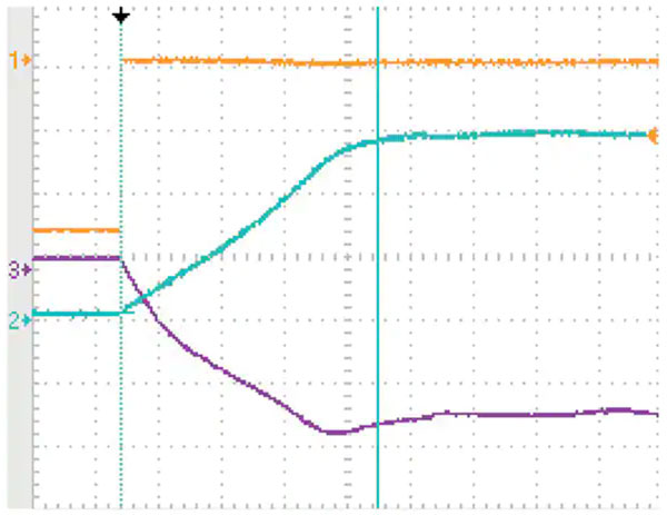
Figure 8: It is critical that the DC/DC converter output remains stable during power-up and power-down sequences without voltage transients. (Image credit: Murata Power Solutions)
• Isolation and Coupling Capacitors: At high power, power inverters or converters typically use a bridge configuration to generate line frequency AC, or to provide bidirectional PWM drive to motors, transformers, or other loads. For user safety and regulatory compliance, the gate drive PWM signal and the associated drive power rails of the high side switches need to be galvanically isolated from ground without any resistive path between them. In addition, the isolation barrier must be very strong and durable without significant performance degradation due to repeated partial discharge effects over the design life.
In addition, there are problems due to capacitive coupling across the isolation barrier; this is similar to leakage current between the primary and secondary windings of a fully insulated AC line transformer. This requires the drive circuit and associated power rails to be immune to high dV/dt at the switch node and have very low coupling capacitance.
The mechanism for this problem is that due to very fast switching speeds, dV/dt is typically as high as 10 kV/μs, and for the latest GaN devices, even as high as 100 kV/μs. This fast swinging dV/dt causes instantaneous current to flow through the capacitance of the DC/DC converter isolation barrier.
Because of the current I = C x (dV/dt), even a small isolation capacitance of only 20 pF will generate a current of 200 mA at 10 kV/μs switching. This current can find an indeterminate return route through the controller circuit back to the bridge, causing voltage spikes across the connecting resistors and inductors that can potentially disrupt the operation of the controller or even the DC/DC converter. Therefore, low coupling capacitance is very important.
There is another problem with basic isolation and associated insulation of DC/DC converters. The isolation barrier is designed to withstand the rated voltage continuously, but due to the switching voltage, the isolation barrier has the potential to degrade rapidly over time. This is because of the electrochemical and partial discharge effects in the barrier material, which are completely dependent on the fixed DC voltage.
Therefore, DC/DC converters must have reliable insulation and generous minimum creepage and clearance distances. If the converter isolation barrier also forms part of the safety isolation system, the relevant agency regulations regarding the required isolation level (basic, supplemental, reinforced), operating voltage, degree of pollution, overvoltage category and altitude apply.
For these reasons, only gate drive DC/DC converters with proper design and materials can pass or apply for UL60950-1 certification, providing various levels of basic and enhanced protection (usually equivalent to the protection in EN 62477-1:2012 level); more stringent certifications are also in place or pending to meet the requirements of medical standard ANSI/AAMI ES60601-1 for 1 × Measures of Patient Protection (MOPP) and 2 × Measures of Operator Protection (MOOP).
• Common Mode Transient Immunity: At higher switching frequencies, where a differential voltage exists between two independent ground references of the gate driver, CMTI is an important gate driver parameter, isolated gate This is the case with drives. CMTI is defined as the maximum allowable rise or fall rate of a common-mode voltage applied between two isolated circuits, and is measured in kV/μs or V/ns.
Having a high CMTI means that both ends (transmit and receive) of the isolated deployment will be out of spec when “slamming” the isolation barrier with a signal that has a very high rising (positive) or falling (negative) slew rate book specifications. The data sheet of the DC/DC converter should contain the specification value of this parameter, and the designer needs to match it according to the specific conditions of the operating frequency and voltage of his circuit.
Meets requirements for gate driver DC/DC converters
Recognizing the many challenging and often conflicting demands placed on gate drive DC/DC converters, Murata has expanded its MGJ2 series of through-hole DC/DC converters to include SMD DC/DC units. Their converters are ideal for space and weight constrained applications due to their high performance, compact form factor and low profile (approximately 20 mm long x 15 mm wide x 4 mm high) and compatible with SMD manufacturing processes Powers the high-side and low-side gate drive circuits for IGBTs and MOSFETs (Figure 9).
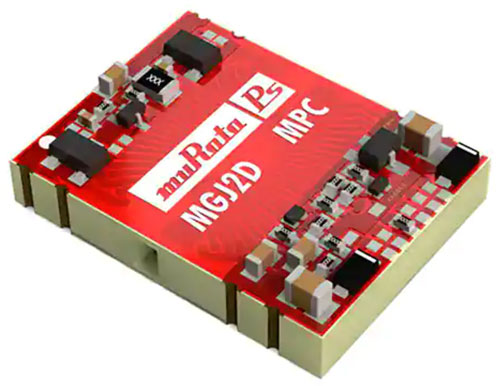
Figure 9: All units of Murata’s MGJ2 series of DC/DC converters have the same appearance and size, but offer a variety of nominal input voltage and bipolar output voltage pairings. (Image credit: Murata Power Solutions)
Members of this family of 2 W converters operate with 5 V, 12 V, and 15 V nominal input voltages and offer asymmetric output voltage options (+15 V/-5 V, +15 V/-9 V, and +20 V/ -5 V output) to support optimal drive levels with the highest system efficiency and least electromagnetic interference (EMI). Surface mount packaging simplifies physical integration with gate drivers, enabling tighter layouts, reducing routing complexity while minimizing EMI or radio frequency interference (RFI) pickup.
The MGJ2 series is specified to meet the high isolation and dV/dt requirements required for bridge circuits used in motor drives and inverters, and its industrial temperature rating and construction provide long life and high reliability. Other key attributes include:
・ Reinforced insulation, meets UL62368 certification requirements (pending)
・ ANSI/AAMI ES60601-1 certification (pending)
・ 5.7 kV DC insulation test voltage (according to “High Voltage Test”)
・ Ultra-low isolation capacitance
・ Operating temperature up to +105°C (derating)
· Short circuit protection
・Characterized Common Mode Transient Immunity (CMTI) >200 kV/μs
・ 2.5 kV continuous isolation withstand voltage performance
・ Characterized partial discharge performance
The following two units demonstrate the range of performance that the MGJ2 series can offer:
• The MGJ2D152005MPC-R7 accepts a nominal 15 V input (13.5 V to 16.5 V) and provides highly asymmetric +20 V and -5.0 V outputs with up to 80 mA each. Key specifications include: 9% and 8% load regulation (max) on both outputs, less than 20/45 mV (typ/max) ripple and noise, and 71/76% (min) efficiency /typ), the isolation capacitance is only 3 pF, and the mean time to failure (MTTF) is approximately 1100 kHr (determined using MIL-HDBK-217 FN2) and 43,500 kHr (calculated according to Telecordia SR-332 model).
• The MGJ2D121509MPC-R7 takes a nominal 12 V input voltage (10.8 V to 13.2 V) and provides asymmetrical +15 V and -9.0 V outputs, also up to 80 mA each. Other key specifications include: +15 V output with 8%/13% load regulation (typ/max), -9.0 V output with 7%/12% load regulation (typ/max), ripple Wave and noise below 20/45 mV (typ/max), 72/77% efficiency (min/typ), 3 pF isolation capacitance, MTTF ~1550 kHr (using MIL-HDBK-217 FN2 OK) and 47,800 kHr (according to the Telecordia model).
In addition to expected lists and graphs detailing static and dynamic performance, the general data sheets for members of this family list the many industry standards and regulatory requirements to which these converters conform, as well as comprehensive details of the associated test conditions used to determine these factors . This not only increases product credibility, but also accelerates product certification in applications with stringent compliance requirements.
Summarize
Selecting the appropriate MOSFET or IGBT device for a switching power supply design is an important step in the design process. In addition, the associated gate driver is selected to control the switching device to toggle between on and off states quickly and neatly. In turn, the drive needs a suitable DC/DC converter to provide it with operating power. As previously shown, Murata’s MGJ2 series of 2 W surface mount DC/DC converters not only provide the required electrical performance, but also meet the many complex safety and regulatory requirements required for this function.