

Content last revised on September 23, 2026
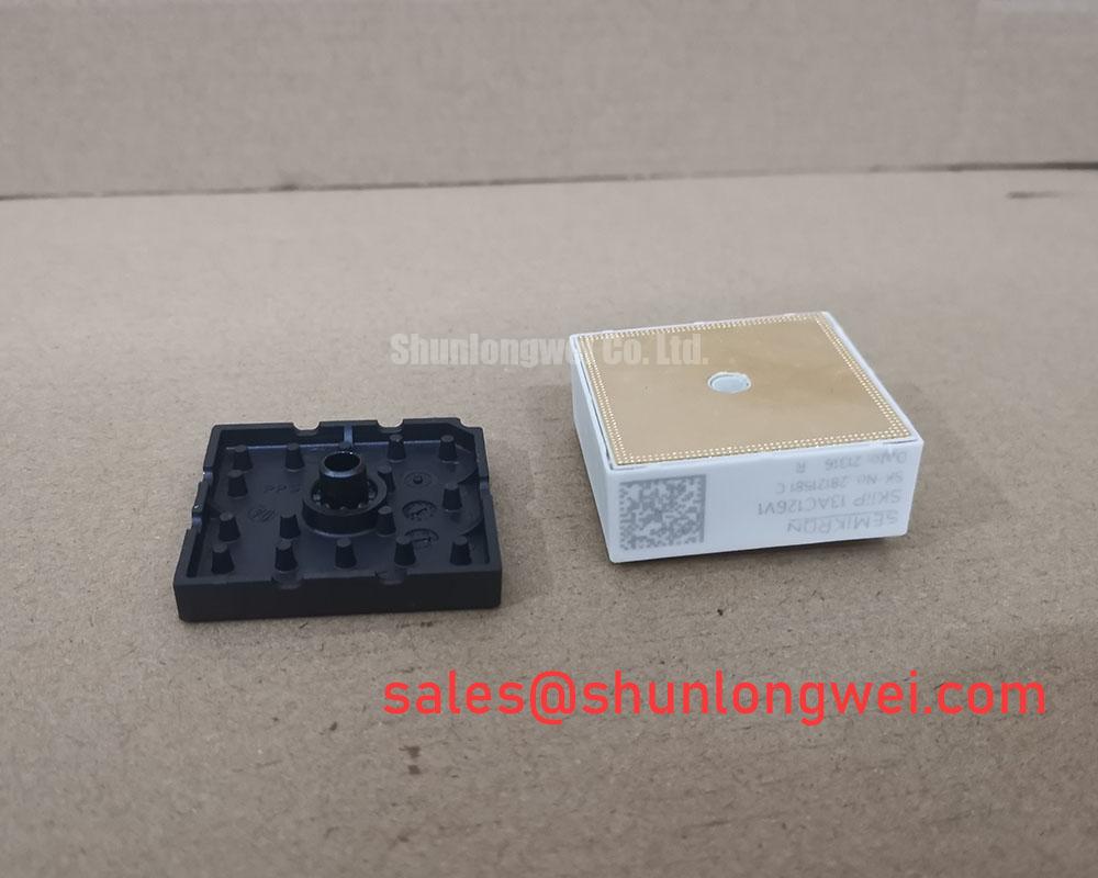
Transient Dynamics & Electrical Design: Dynamic Power Loss Dissipation and Multi R on SKIIP 13AC126V1
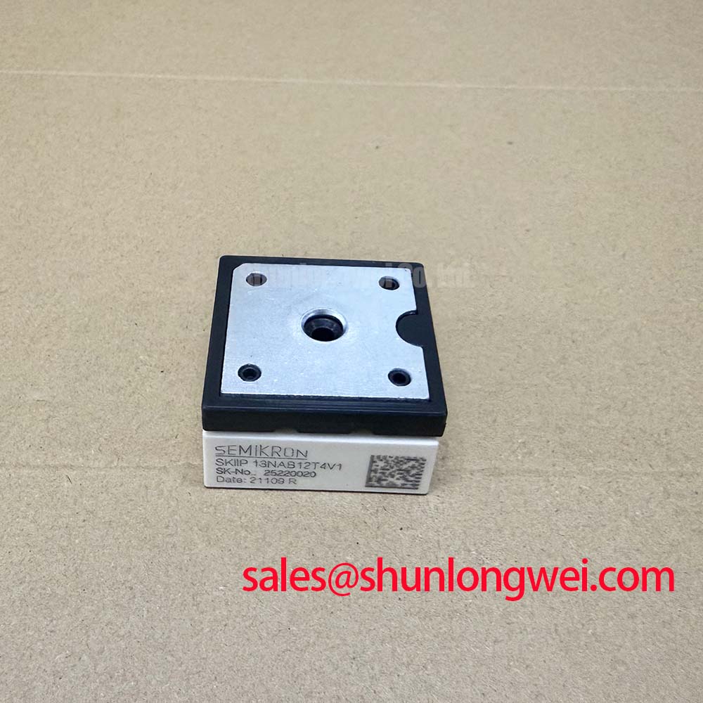
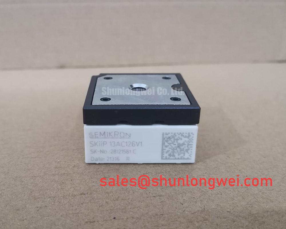
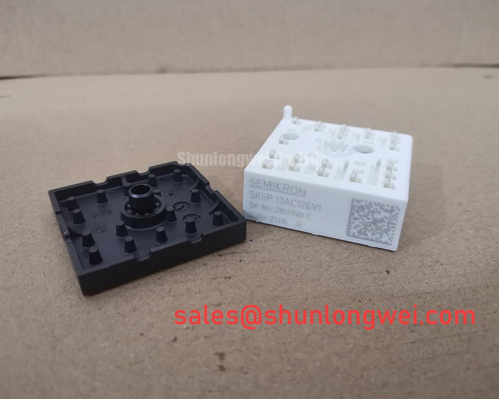
The SKIIP 13AC126V1 should be assessed as a complete power module within its original converter arrangement, rather than as an isolated switching die. During repetitive acceleration, load changes, or stalled axis investigation, junction temperature can rise faster than the external heatsink response suggests. A multi resistance thermal network is commonly used by designers to represent the time dependent path from semiconductor junction through the case and thermal interface into the heatsink. This is a Design Consideration, not a published thermal model or guaranteed transient rating for this exact module.
For a pulsed load assessment, the engineering calculation must combine measured or datasheet supported conduction and switching losses with the applicable transient thermal impedance curve and the measured case temperature. Without the original Semikron thermal curves, switching conditions, and cooling assembly information, a reliable peak junction temperature calculation cannot be stated for this model. Maintenance engineers should therefore preserve the original fan path, heatsink condition, thermal interface arrangement, and control timing before attributing a trip event to the IPM itself.
Inspect the mounting face for old compound buildup, scratches, burrs, bowed metalwork, and uneven clamp pressure. A thin, continuous thermal interface layer is a general assembly principle because voids can locally restrict heat flow. The final mounting method must follow the host equipment documentation and the applicable fastener specification.
⚠️ Field Alert: Disconnect control power and discharge the DC link before removing module connections, because a retained bus charge or unintended drive command can damage the replacement module and connected equipment.
Layout work also matters when a repaired drive returns with intermittent overcurrent or thermal warnings. Keep power conductors arranged to reduce loop area, separate sensitive gate and feedback wiring from high current paths, and confirm that terminal hardware is fully seated. These are Engineering Recommendations intended to reduce parasitic effects during switching; the system engineer must verify electrical clearance, creepage, and peak operating stress against the actual converter voltage and enclosure conditions.
For broader context on integrated power module construction and product family positioning, consult the Semikron MiniSKiiP® power module information. The source should be read alongside the original equipment circuit documentation because a family description does not replace model specific terminal and operating data.
Benchtop Waveform Tuning: Mitigating Stress via Regenerative DC Bus Voltage Surge Dissipation on SKIIP 13AC126V1
Before reconnecting a drive after replacement, trace where regenerative motor energy is expected to go during deceleration. In a light industrial automation cabinet or a multi joint robotic articulator, the mechanical load can return energy to the DC bus when an axis slows. The system may use a braking path, a shared energy bus, or another manufacturer defined energy management method. The 1200.0 V device rating is an Official Datasheet Specification, but it does not by itself define the acceptable DC bus setting, braking resistor value, braking duty cycle, or regenerative energy capacity of the complete machine.
On the bench, observe the bus voltage and relevant control command with properly rated differential measurement equipment while running the machine through a controlled deceleration sequence. A rising bus waveform may point toward disabled braking control, an open resistor circuit, unsuitable command timing, poor DC link condition, or a load profile outside the original machine assumptions. It should not be assigned to a single cause without checking the schematic, parameter set, and connected motor mechanics.
Where the original equipment includes an external braking transistor and ballast resistor, component sizing is a system level calculation based on stored mechanical energy, permitted bus voltage excursion, resistor pulse capability, switching duty, and cooling. This is an Engineering Calculation only when those verified inputs are available. Designers should retain the original braking topology and validate any service change under controlled load testing. It is not appropriate to assign an arbitrary resistor value or a universal braking threshold to the SKIIP 13AC126V1.
Input stage behaviour also deserves attention. In converters that use phase angle control or line rectification, conduction timing can affect line current shape and DC bus ripple. DC link capacitors and their interconnections influence how that ripple reaches the inverter stage. A noisy or distorted waveform can result from input source impedance, capacitor condition, commutation behaviour, measurement setup, or control synchronization. Compare the waveform with the known good signal path and inspect the DC link hardware before changing gate related components.
RC snubbers, when present in the original design, can absorb part of a switching transient. Their capacitance, resistance, voltage class, placement, and dissipation capability must be evaluated against the host converter’s measured ringing frequency and switching energy. This is a Design Consideration. A changed snubber can alter losses and waveform shape, so validation should include both normal operation and the machine’s intended acceleration and deceleration cycles.
For systems where upstream conversion hardware is also under review, SKM100GB063D is a related power semiconductor listing that can be examined against the documented topology. It should not be treated as a drop in substitute for the SKIIP 13AC126V1 without confirming circuit function, control interface, mechanical format, ratings, and protection coordination.
Preventing Spurious Faults: Turn Off di/dt Induced Vpeak Clamping and Guidelines for SKIIP 13AC126V1
A turn off event can create a voltage overshoot because stray inductance resists a rapid current change. In practical terms, peak voltage is influenced by DC bus voltage plus the product of parasitic loop inductance and current slew rate. This Engineering Calculation relationship explains why cable routing, busbar geometry, terminal contact quality, and snubber placement can affect measured stress even when the module marking is unchanged.
Use an oscilloscope measurement arrangement suitable for high voltage switching work and keep the probe connection method repeatable. Long measurement leads can add their own loop inductance and make ringing appear worse or different from the actual module terminal waveform. Compare DC bus voltage, phase voltage, gate command behaviour, and fault timing during a controlled test. If a fault appears only at a particular motion profile, check whether current regulation, bus recovery, braking activity, and gate drive response remain consistent through that event.
Minimizing the commutation loop is an Engineering Recommendation intended to suppress turn off overshoot. The required busbar geometry, conductor spacing, snubber location, and permissible current slew rate are system determined. The system engineer should verify measured peak voltage margins against the actual DC link condition during switching tests, while respecting the Official Datasheet Specification of 1200.0 V for this module.
Fast semiconductor fuses can be part of a coordinated protection strategy in equipment designed for them. Their I²t characteristic, interruption rating, cable contribution, fault clearing sequence, and interaction with the converter protection must be matched to the original system design. A fuse should not be selected only from the module’s 13.0 A rated current, because normal operating current and short circuit protection coordination are different engineering questions.
When service documentation calls for a module with the same family style but a different documented electrical capability, the SKIIP37AC12T4V1 listing can be reviewed as a separate compatibility candidate. Its use requires confirmation of the original circuit topology, mounting arrangement, terminal mapping, drive interface, protection settings, and thermal design. A higher current marking alone does not establish functional interchangeability.
SKIIP 13AC126V1 Operational Boundaries: Evaluating Common-Mode Transient Immunity Under Harsh Conditions
Common mode switching activity can disturb low voltage control circuits through coupling paths in gate drive wiring, current feedback paths, auxiliary supplies, and measurement equipment. The supplied official product identity for the SKIIP 13AC126V1 confirms a Semikron SKiiP package family with 1200.0 V and 13.0 A ratings. It does not provide a verified model specific reinforced isolation rating or common mode transient immunity value. Those figures must not be assumed from package family descriptions.
When a repaired axis drive gives irregular gate related trips, inspect connector locking, shield termination, grounding continuity, auxiliary supply stability, and separation between power and control harnesses. Look for waveform correlation between switching edges and the reported fault input. Such correlation may indicate common mode coupling or measurement sensitivity, but it should be verified against the known good signal path rather than treated as proof of a single defect.
Designers evaluating isolation barriers should use the original module datasheet, drive board documentation, and applicable equipment safety requirements to establish required insulation coordination. Physical separation, controlled return paths, correctly terminated shields, and clean control supply references are Design Considerations that can reduce unwanted coupling. Final limits depend on the host installation, switching waveform, enclosure, maintenance condition, and machine level protection architecture.
The Semikron Danfoss SKiiP® technology information provides useful family level context for integrated power solutions. For application level discussion of power semiconductor deployment, see Industrial Applications. Both resources should support, rather than replace, direct verification against the original equipment documentation and measured operating waveforms.