Shunlongwei Co. ltd.
IGBT Module / LCD Display Distributor
Customer Service
+86-755-8273 2562
IGBT Module / LCD Display Distributor
“The proliferation of electric vehicles has pushed the boundaries of power semiconductor performance to new heights. Traditionally, silicon power devices have been used to control various power Electronic systems in automobiles, such as for main inverter motors, pumps, HVAC compressors, braking and steering systems. Recent developments in compound semiconductor devices such as silicon carbide (SiC) have made it possible to increase the efficiency of most systems in vehicles. Certain properties of SiC devices, such as low conduction and switching losses, zero recovery body diodes, and higher operating junction temperatures, make this technology ideal for efficiency-critical automotive applications.
“
The proliferation of electric vehicles has pushed the boundaries of power semiconductor performance to new heights. Traditionally, silicon power devices have been used to control various power electronic systems in automobiles, such as for main inverter motors, pumps, HVAC compressors, braking and steering systems. Recent developments in compound semiconductor devices such as silicon carbide (SiC) have made it possible to increase the efficiency of most systems in vehicles. Certain properties of SiC devices, such as low conduction and switching losses, zero recovery body diodes, and higher operating junction temperatures, make this technology ideal for efficiency-critical automotive applications.
For nearly 20 years, silicon-based IGBTs have become the device of choice in 300V to 1000V medium voltage automotive applications. SiC technology addresses the same automotive applications as IGBTs, with advantages such as lower conductivity, lower switching losses and higher thermal conductivity compared to IGBT technology. Figure 1 shows the forward characteristic comparison of IGBT and SiC Mosfet. SiC Mosfets behave like a resistor, with a voltage drop proportional to the current flowing through the device. An IGBT is a minority carrier device with a PN junction that behaves like a diode with a typical voltage drop across the device of 0.7V regardless of the current flowing through the device.

Figure 1: Forward characteristics of SiC Mosfet and IGBT. The SiC Mosfet behaves like a resistor, while the IGBT has a fixed 0.7V PN junction drop.
In addition, the switching characteristics and losses of SiC Mosfet are independent of chip temperature. As the junction temperature of SiC Mosfet increases, its switching loss remains constant, which enables SiC Mosfet to have higher operating current capability than IGBT. For IGBTs, an increase in junction temperature will slow down the device, which will further increase its switching losses. These phenomena will limit the operating current of the IGBT to be lower than that of a SiC Mosfet of similar size. Figure 2 illustrates the current switching behavior of the SiC Mosfet and the IGBT, showing that the switching time and peak current of the IGBT increase, while these two quantities remain constant for the SiC Mosfet.

Figure 2: Switching current characteristics of IGBTs vary with temperature while SiC Mosfet is constant.
The second most important improvement that SiC technology can bring is on-board charger (OBC) applications for electric vehicles. Here, the SiC Mosfet enables the most efficient totem-pole power factor correction (PFC) topology by eliminating the traditional line frequency rectifier from the design. This topology is also well suited to the needs of bidirectional power flow, and in the future, certain regions and municipalities will require vehicles to deliver energy back to the grid. The converter downstream of the PFC is the CLLC DC/DC converter, which is connected to the vehicle propulsion battery. Here, both the primary and secondary sides of the DC/DC converter can greatly benefit from SiC devices. Figure 3 illustrates the bidirectional OBC topology realized by introducing SiC Mosfets.
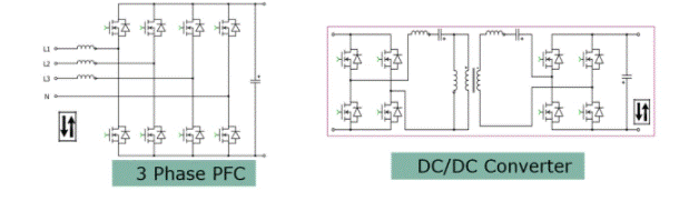
Figure 3: Three-phase totem-pole PFC followed by a full-bridge CLLC for bidirectional OBC enabled by SiC Mosfet technology.
Device packaging is also an important topic. Traditional through-hole devices in TO247 have become standard in many OBC designs. However, assembly automation requires surface mount devices (SMDs) with proper package creepage and clearance to keep costs down. Using SMD equipment, the entire printed circuit board assembly with power supply unit can be assembled in one step. The latest PG-TO263-7pin package with high creepage and Kelvin source connection solves the problem of 1200V SiC Mosfet. The PG-TO263-2pin package is suitable for SiC diode devices where the middle pin has been completely removed to address creepage requirements.
Additionally, top-side cooling surface mount devices will further improve SiC device performance by reducing thermal resistance from package to cooler while simplifying power device assembly. The PG-HDSOP-22 (QDPAK) package is an innovative package from Infineon that perfectly meets top heat dissipation requirements. The QDPAK is available in a surface mount package and offers Kelvin source connections and high creepage distances. As the current increases, it is also planned to adopt the same standard of TO247-4pin, which is to provide Kelvin source and high creepage distance in a package with high current carrying capacity. To complement its SiC Mosfet and diode offerings, Infineon has also made these packages available for traditional silicon technology for IGBTs, diodes and superjunction Mosfets. From the standpoint of efficiency, cost and ease of assembly, this will provide a complete solution for OBC applications.
Figure 4 shows an innovative software package from Infineon for OBC applications. The QDPAK is available in a surface mount package and offers Kelvin source connections and high creepage distances. As the current increases, it is also planned to adopt the same standard of TO247-4pin, which is to provide Kelvin source and high creepage distance in a package with high current carrying capacity. To complement its SiC Mosfet and diode offerings, Infineon has also made these packages available for traditional silicon technology for IGBTs, diodes and superjunction Mosfets. From the standpoint of efficiency, cost and ease of assembly, this will provide a complete solution for OBC applications.
Figure 4 shows an innovative software package from Infineon for OBC applications. The QDPAK is available in a surface mount package and offers Kelvin source connections and high creepage distances. As the current increases, it is also planned to adopt the same standard of TO247-4pin, which is to provide Kelvin source and high creepage distance in a package with high current carrying capacity. To complement its SiC Mosfet and diode offerings, Infineon has also made these packages available for traditional silicon technology for IGBTs, diodes and superjunction Mosfets. From the standpoint of efficiency, cost and ease of assembly, this will provide a complete solution for OBC applications. Figure 4 shows an innovative software package from Infineon for OBC applications. To complement its SiC Mosfet and diode offerings, Infineon has also made these packages available for traditional silicon technology for IGBTs, diodes and superjunction Mosfets. From the standpoint of efficiency, cost and ease of assembly, this will provide a complete solution for OBC applications. Figure 4 shows an innovative software package from Infineon for OBC applications. To complement its SiC Mosfet and diode offerings, Infineon has also made these packages available for traditional silicon technology for IGBTs, diodes and superjunction Mosfets. From the standpoint of efficiency, cost and ease of assembly, this will provide a complete solution for OBC applications. Figure 4 shows an innovative software package from Infineon for OBC applications.
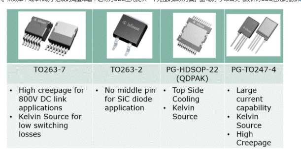
Figure 4: Infineon innovation kit for OBC applications
The Links: SKMD150F12 NL8060BC21-03