Designers of instrumentation and measurement systems require low-jitter, spurious-free signals to deliver the required signal-to-noise ratio (SNR) or error vector magnitude (EVM) to meet increasingly demanding customer requirements. At the same time, they are under enormous pressure to reduce board area and design cost and complexity. The latter is critical to reducing development time to meet ever-shrinking time-to-market windows.
Designers of instrumentation and measurement systems require low-jitter, spurious-free signals to deliver the required signal-to-noise ratio (SNR) or error vector magnitude (EVM) to meet increasingly demanding customer requirements. At the same time, they are under enormous pressure to reduce board area and design cost and complexity. The latter is critical to reducing development time to meet ever-shrinking time-to-market windows.
To address numerous application challenges, engineers need to transition their instrumentation and measurement clock solutions from traditional custom discrete designs to more integrated solutions. An important step in achieving this is the use of an integrated translation phase-locked loop (PLL). It allows conventional voltage-controlled oscillator (VCO) signals to be frequency upconverted while substantially maintaining the jitter and phase noise of a fixed external local oscillator (LO).
This article discusses the role of the translation loop in achieving the industry’s lowest integrated phase noise. By way of example, this article introduces Analog Devices’ ADF4401A translation ring system-in-package (TL SiP) and shows how it meets performance requirements with sub-10 femtosecond (fs) rms wideband combined jitter capability and enhanced isolation of the output signal requirements, while also meeting the designer’s integration, cost, complexity and time-to-market needs.
Traditional PLL and translation loop operation
The main purpose of the translation loop is to generate an output signal locked to the input reference signal with greatly reduced in-band phase noise compared to conventional PLLs.
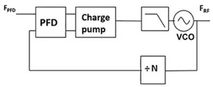
A standard PLL consists of a feedback system consisting of a phase frequency detector (PFD), charge pump, low pass filter (LPF), VCO, and a feedback divider N (Figure 1).

Figure 1: A standard PLL locks to a lower frequency (FPFD) reference and produces an output frequency (FRF). (Image credit: Bonnie Baker)
The PFD compares the phase of the input reference signal with the phase of the feedback signal and generates a series of pulses proportional to the phase error between them. The charge pump receives the PFD pulses and converts them into current source or current sink pulses, which in turn adjust the frequency of the VCO to rise or fall. The LPF removes the high frequency energy of all pulses and converts it into a voltage that the VCO can use. The output signal of the VCO is fed back to the PFD block through the N divider to complete the loop.
The frequency transfer function of Figure 1 is calculated using Equation 1.
![]() Equation 1
Equation 1
where FRF is the output frequency
N is the ratio of the feedback divider (can be integer or fractional).
FPFD is the PFD frequency
The in-band noise floor of Figure 1 is calculated using Equation 2.
![]() Equation 2
Equation 2
where FOMPLL is the in-band phase noise floor figure of merit (FOM) of the PLL
Consider an example where the in-band phase noise floor FOM is -234 decibels per hertz (dB/Hz); the PFD frequency (FPFD) is 160 megahertz (MHz) and the output frequency (FRF) is 8 gigahertz (GHz).
For this system, Equation 1 is used to calculate the value of N:

Equation 2 is used to calculate the in-band noise floor:

In the calculations above, the N divider contributes 20log10(50) to the overall in-band noise floor, which equates to 34dB. Smaller values of N reduce the in-band noise floor; however, it also reduces the output frequency. So how do we generate a high output frequency and keep the loop gain (N) low?

Figure 2: For the standard PLL in this example, the noise of the feedback divider (20log10(N)) is 34dB higher than the in-band noise compared to the yellow lower graph with N=1. (Image credit: Bonnie Baker)
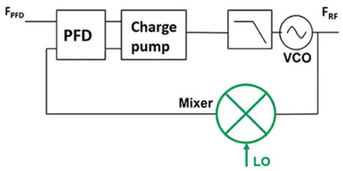
The solution to this problem is to replace the N divider with a downconversion mixing stage (Figure 3).

Figure 3: The translation loop uses a mixer to down-convert the VCO frequency to the PFD frequency instead of using a traditional feedback divider. (Image credit: Bonnie Baker)
In Figure 3, the mixer replaces the feedback-N divider, resulting in a loop gain equal to 1 (N=1). This operation will greatly reduce the feedback loop’s effect on the in-band noise floor. The value of N is now equal to 1 for in-band noise calculations. Using Equation 2, the in-band noise floor of the modified system is as follows. :

The new in-band noise shows a 34dBc/Hz improvement.
In Figure 3, the mixer relies on a very low noise LO, called the offset LO. FLO ± FRF must equal FPFD to achieve lock.
In a translation loop configuration, the phase noise of the offset LO is important for optimal performance at the RF output. For this reason, engineers typically design an offset LO based on a voltage-controlled surface acoustic wave (SAW), or oscillator (VCSO), or comb generator, or dielectric resonator (DRO). Note: Contact Analog Devices for design support for offset LOs.
The challenge of panning the ring
Traditionally, the design of low-noise translation loops involves the implementation of numerous circuit blocks, resulting in complex designs that are often bulky and have limited flexibility. Additionally, the entire circuit must be verified and characterized for target operation. For example, a major design concern is LO leakage to the RF output signal (LO from RF isolation). This is a major challenge for engineers to solve. With traditional designs, engineers typically perform multiple design iterations to achieve optimized performance and proper isolation.
Figure 3 shows how the ADF4401A integrates the main circuit blocks to provide a fully characterized solution and eliminate the difficult areas traditionally associated with performance and isolation in translation ring designs. This programmable solution enables engineers to achieve optimized performance on the first try and accelerate time to market.
Evaluating the ADF4401A
The ADF4401A is designed to help engineers reduce the time to market for high-performance instruments using frequency generation solutions with RF bandwidths from 62.5 MHz to 8 GHz. Using a downconversion mixer, the ADF4401A has very low in-band noise, with a wideband jitter of about 9 femtoseconds (fs) from 100 Hz to 100 MHz. Design and layout techniques within the ADF4401A result in a typical spurious free dynamic range of 90 dBc. The 18 x 18 x 2.018 millimeter (mm) package size significantly reduces board space compared to traditional discrete designs.
To evaluate the performance of this device, designers can use the EV-ADF4401ASD2Z evaluation board (Figure 4). The board includes a complete translation loop including an external PFD (HMC3716), an active filter (LT6200), and a multiplexer (ADG1609).

Figure 4: The EV-ADF4401ASD2Z evaluation board for the ADF4401A translation loop module includes an external PFD, a USB interface, and voltage regulators. (Image credit: Analog Devices)
The EV-ADF4401ASD2Z includes the ADF4401A TL SiP with integrated VCO, a loop filter (5MHz), a PFD, a USB interface, and voltage regulators. Additionally, the EV-ADF4401ASD2Z requires the EVAL-SDP-CS1Z (SDP-S) System Demonstration Platform (SDP) (serial) controller board (Figure 5). The board provides a USB connection from the PC to the EV-ADF4401ASD2Z so it can be programmed. This controller board is not included in the EV-ADF4401ASD2Z kit.

Figure 5: The EVAL-SDP-CS1Z (or SDP-S) controller board is required to provide a USB connection from the EV-ADF4401ASD2Z to the PC for programming. (Image credit: Analog Devices)
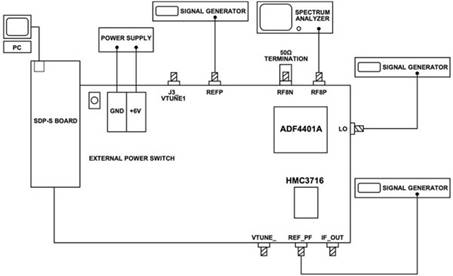
Figure 6 shows the physical connections of the EV-ADF4401ASD2Z system. The Correlation Analysis | Control | Evaluation (ACE) software controls the TL SiP functionality. Power comes from an external 6 volt supply.

Figure 6: The EV-ADF4401ASD2Z installation diagram shows the equipment and connections required to evaluate the ADF4401A, including the SDP-S control board, PC, power supply, signal generator, and spectrum analyzer. (Image credit: Analog Devices)
Recommended equipment for use with this evaluation board includes a Windows PC, a spectrum analyzer or signal source analyzer, and three signal generators.
The block diagram of the EV-ADF4401ASD2Z shows the ADF4401A module, along with Analog Devices’ HMC3716 PFD, LT6200 op amp, and ADG1219 SPDT switch (Figure 7).

Figure 7: The EV-ADF4401ASD2Z evaluation board block diagram shows the key components that support the AD4401A translation loop. (Image credit: Analog Devices)
Using a PFD capable of operating at high frequencies is critical, as this minimizes the need for crossovers, which reduce in-band noise response. The 1.3 GHz phase comparison frequency capability of Analog Devices’ HMC3716 makes it ideal for use in the IF range of the ADF4401A. This circuit is able to compare frequency and phase simultaneously, so no additional circuitry is required to steer the frequency to a predetermined output frequency. The HMC3716 becomes an external PFD, completing the offset loop. The high frequency operating range and ultra-low phase noise floor of the HMC3716 make it possible to design wideband loop filters.
In Figure 7, the LT6200 op amp in an LPF configuration attenuates high frequency spikes, while the ADG1219 switch completes the system’s translation loop.
Figure 8 shows the in-band noise plot and jitter measurement produced by the EV-ADF4401ASD2Z evaluation board.

Figure 8: SSB phase noise at 5 GHz output with external HMC3716 reference at 500MHz and external LO at 4.5GHz. (Image credit: Analog Devices)
In Figure 8, the LO2 and HMC3716 inputs are an SMA100B RF and microwave signal generator. The LO2 in-band noise of this evaluation board is about -135 dBc/Hz, which is noticeable at low offsets up to 300kHz. The in-band noise from the LO2, ADF4401A module, HMC3716 PFD and loop filter is approximately -140 dBc/Hz. Internal phase noise occurs between 5MHz and 50MHz, and the evaluation board’s phase noise floor is approximately -160dBc/Hz. Together these factors add up to an rms jitter of 12.53 fs.
Epilogue
High-speed instrumentation systems require extremely low-jitter clocks to ensure that output data is not affected. The challenge for engineers is to find the right equipment that can build high-speed gigahertz clocking systems. The ADF4401A translation ring greatly simplifies device selection for building clocking systems, providing a compact module that ensures low jitter at higher frequencies while reducing board space, cost, and time-to-market.
(Source: China Power Grid, Author: Bonnie Baker)
The Links: LM150X08-B5 SKM400GAL124D