

Content last revised on September 18, 2026
Field Diagnostics & Commissioning: Thermal Interface Material Thickness Uniformity in SKIIP32NAB12T7 Topologies
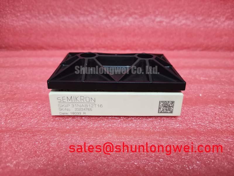
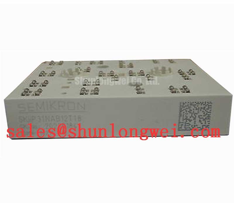
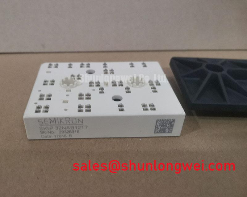
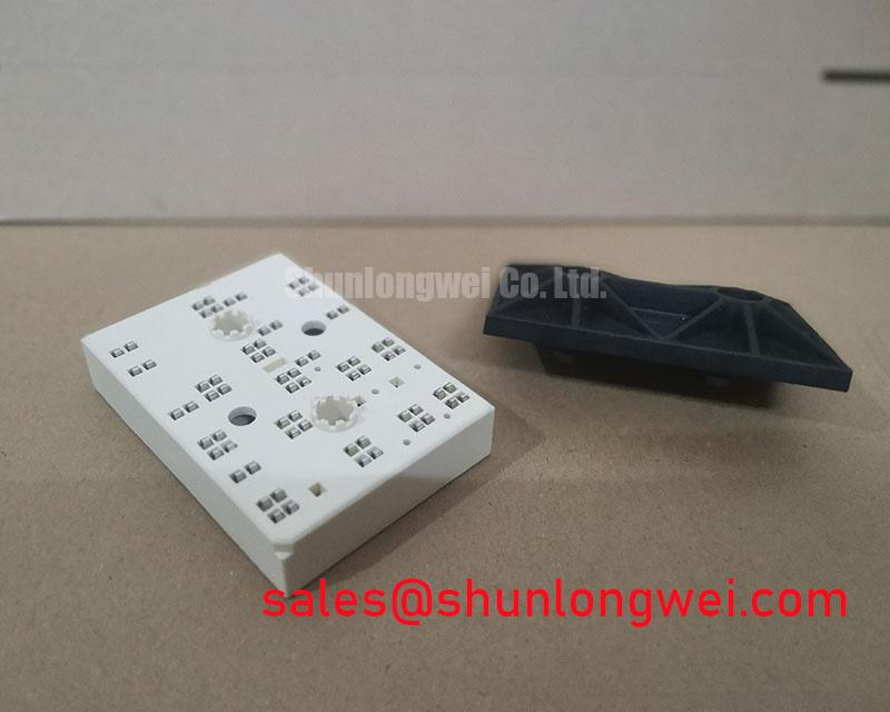
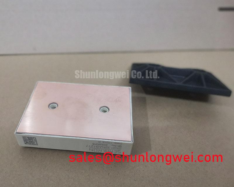
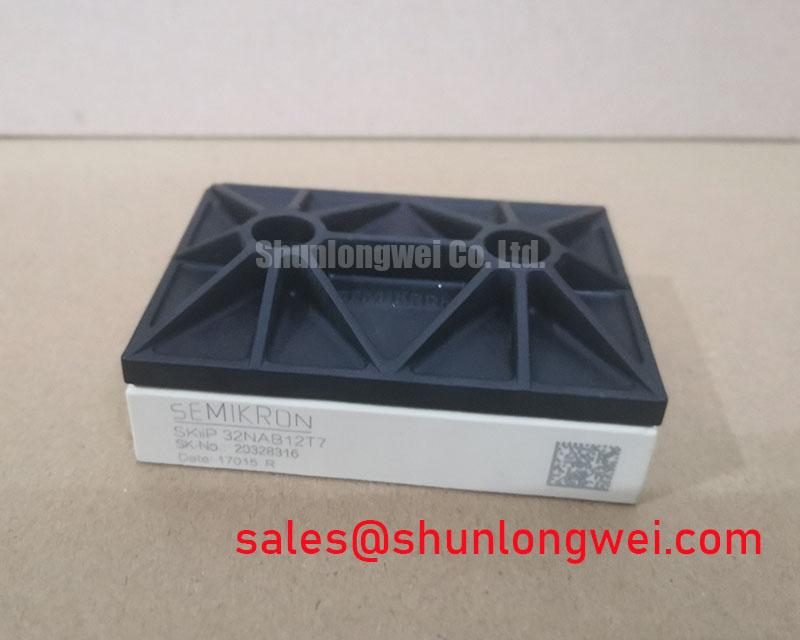
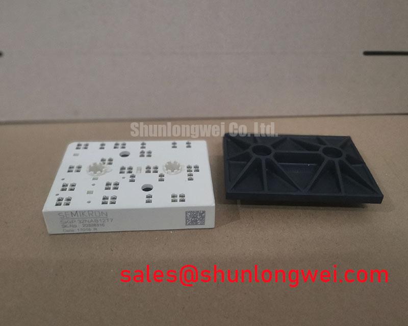
Before energizing a replacement drive, verify the nameplate boundary against the control cabinet documentation and inspect the heatsink contact area for trapped debris, corrosion, damaged insulation hardware, or uneven remnants of the previous thermal compound. The SKIIP32NAB12T7 is a Semikron power module in the MiniSKiiP / SKiiP package family, rated at 1200 V and 32 A as an Official Datasheet Specification. These ratings establish the electrical identity of the unit, but they do not alone confirm suitability for a particular inverter, servo axis, or automation controller. The original equipment circuit, gate-drive arrangement, cooling path, DC-link condition, and fault-protection coordination should all be checked before commissioning.
| Manufacturer | Semikron |
| Product model | SKIIP32NAB12T7 |
| Voltage rating | 1200 V Official Datasheet Specification |
| Current rating | 32 A Official Datasheet Specification |
| Package family | MiniSKiiP / SKiiP |
| Product category | Intelligent Power Module |
For equipment repair teams, the practical task is to preserve the electrical and thermal conditions that the original module experienced. A correct part number and matching voltage class are necessary checkpoints, while terminal assignment, control-interface behavior, insulation arrangement, and cooling hardware must be confirmed from the original system documentation. Semikron’s MiniSKiiP power module information provides useful family-level context, but an installed control assembly should always be evaluated as a complete switching system.
The first thermal check is performed with the system isolated, discharged, and mechanically accessible. Remove old interface material from the heatsink using an approved cleaning process, then inspect the mounting plane under angled light. Raised burrs, hardened compound, embedded particles, or a visibly bowed mounting surface can prevent uniform heat transfer even when the fasteners appear secure. Because the SKIIP32NAB12T7 carries a 32 A official current rating, a localized thermal interface defect can become important during repeated switching or sustained load operation.
A thermal interface layer should fill microscopic surface variation without becoming a thick thermal barrier. A layer in the general range of 50 to 100 µm is a Design Consideration commonly used when the selected interface material and mounting geometry support that thickness. It is not an official thickness requirement for this specific Semikron module. The equipment integrator should follow the interface-material supplier guidance and verify the result by examining compound spread after an initial controlled fit. A dry region, a heavy ridge at one edge, or a pattern that suggests one corner is carrying most of the clamping load indicates that the contact stack needs further inspection.
Baseplate curvature and heatsink flatness must be considered together rather than judged separately. A heatsink that has been repeatedly thermally cycled can develop localized distortion near threaded holes or around a prior module footprint. When reusing a cabinet assembly, compare the cleaned mounting plane with a known reference surface where practical. Do not compensate for a damaged heatsink with an excessive quantity of compound. That approach can conceal the mechanical issue while increasing thermal resistance and making future inspection harder.
Mounting screws should be engaged progressively in a balanced sequence so that the module settles against the heatsink without being pulled down unevenly from one side. The final torque is system-dependent and must follow the hardware and module documentation used by the original equipment manufacturer. ⚠️ Maintenance Note: After the first loaded thermal cycle, monitor heatsink contact temperature trends and recheck that cooling-air paths remain clear before returning the equipment to unattended service.
During commissioning, compare temperature behavior across equivalent operating states rather than relying on a single surface reading. A hotter-than-expected region may be related to the thermal interface, a restricted fan path, inaccurate current feedback, altered switching conditions, or an upstream DC-link issue. It should be investigated through controlled measurements. In light industrial automation and multi-joint robotic articulator drives, periodic cleaning of fan guards, duct channels, and heatsink fins helps prevent temperature drift caused by airborne dust. Where a cabinet experiences humidity changes, inspect for condensation risk around power terminals and adjacent control boards before applying power.
Field Diagnostics & Commissioning: High dv/dt Cross-Conduction Shoot-Through in SKIIP32NAB12T7 Topologies
High switching-voltage transition rates can couple energy into gate-control paths and may disturb the intended off-state of a complementary switching device. This is a Design Consideration for inverter assemblies using the SKIIP32NAB12T7; it is not evidence of a module defect by itself. When unexplained DC-link current spikes, abnormal audible noise, or irregular gate waveforms are observed, evaluate the entire gate-drive loop with suitable differential measurement equipment and compare it against a known-good signal path where available.
The key inspection point is the separation between the power-current return path and the gate-driver reference path. Shared impedance can convert power-current changes into gate-reference movement, which can reduce the effective turn-off margin. Designers commonly assess dedicated low-impedance active Miller-clamp arrangements and controlled negative gate-bias schemes to resist unintended turn-on during rapid switching transitions. The applicable gate voltages, drive resistance, timing, and clamp implementation must be taken from the original drive design and verified against the module documentation. They cannot be safely prescribed from the 1200 V and 32 A nameplate ratings alone.
Field repair work should also examine the driver supply rails, isolators, gate connectors, return traces, and any local decoupling components for signs of heat stress or mechanical damage. A gate signal that appears correct at an unloaded controller connector can behave differently when the power circuit is active. Measurements should therefore be performed with appropriate safety controls and at operating conditions that allow the service team to observe switching behavior without exceeding the established equipment limits.
Protection coordination deserves separate attention. A high-speed semiconductor fuse is selected at system level by relating its clearing behavior and I²t capability to the prospective fault current, the DC-link energy available, the semiconductor surge capability stated in applicable documentation, and the protection architecture. It is not valid to assign a universal fuse size to this module. For a suspected shoot-through event, inspect the fuse, contactors, precharge components, busbar joints, and DC-link capacitors as a linked fault path. A cleared fuse may isolate a downstream fault, but it does not establish the original trigger mechanism.
Freewheel behavior, reverse-recovery characteristics, and resulting conducted or radiated noise are also system-dependent. The reverse-recovery softness factor, where available in the relevant device documentation, can assist waveform interpretation, but it should not be used alone to predict electromagnetic compatibility. A power module cannot independently certify compliance with equipment-level EMC standards. Cable routing, enclosure bonding, filter design, grounding strategy, switching frequency, and measurement configuration remain part of the complete machine assessment.
Transient Dynamics & Electrical Design: DC-Link Capacitance Bank Layout and Low-ESL Control on SKIIP32NAB12T7
When a switching device turns off, the voltage observed by the power stage is influenced by the DC-link voltage plus the inductive contribution created by current change through the commutation path. In engineering terms, peak voltage rises as loop inductance and switching current slope increase. This is an Engineering Calculation principle expressed by the relationship between DC-link voltage, parasitic inductance, and current-transition rate. The actual peak must be verified by measurement at the assembled inverter because wiring length, capacitor placement, busbar geometry, probe method, and operating load all affect the result.
For the SKIIP32NAB12T7, keep the DC-link capacitor connection physically close to the relevant power-current path where the original equipment topology permits. The objective is to minimize parasitic loop inductance and reduce turn-off overshoot, with final peak-voltage margins verified during switching tests against the actual DC-link voltage. A symmetrical planar busbar arrangement is often evaluated in industrial power stages because paired forward and return conductors can reduce loop area. Its usefulness depends on the full mechanical layout, insulation spacing, terminal geometry, and service accessibility.
Do not judge a capacitor bank solely by capacitance value. Equivalent series resistance, current capability, temperature condition, mechanical connections, and the condition of parallel capacitors can influence ripple behavior and transient response. Aged capacitors may present increased heating, altered waveform quality, or inconsistent voltage behavior, although each symptom requires measurement before a cause is assigned. During preventive maintenance, inspect capacitor terminals for discoloration, looseness, electrolyte evidence where applicable, and strain from heavy cabling or vibration.
Snubber capacitors and clamp networks are selected for a specific switching loop, operating waveform, and protection objective. They should be evaluated with the device voltage boundary and measured transient energy in mind, not added as a generic repair modification. If an existing snubber network is present, confirm its wiring route, capacitor condition, insulation integrity, and connection resistance before changing components. Altering only one element of a proven assembly can move stress into another part of the commutation loop.
In a complete power-conversion chain, the module may operate alongside rectification or DC-link elements with different electrical roles. For reference during architecture review, the SKM100GB063D can be examined as a separate power-module option for related system stages. It is not presented as a direct replacement for the SKIIP32NAB12T7. Pinout, topology, electrical ratings, thermal interface, driver compatibility, and protection behavior must be independently confirmed before any component-level decision.
SKIIP32NAB12T7 Operational Boundaries: Evaluating PCB Symmetry Considerations
Before reconnecting gate-drive wiring, trace the power and control returns separately on the original schematic and PCB layout. In multi-switch power stages, mutual coupling through a shared emitter or return path can alter the voltage seen by the driver during current transitions. This can contribute to oscillation, unexpected switching behavior, or uneven stress between devices. The correct response is a controlled layout review and waveform verification, not an assumption that the SKIIP32NAB12T7 itself is responsible for every irregular gate trace.
A Design Consideration is to keep the auxiliary emitter or gate-driver reference return distinct from the main high-current emitter return until the intended reference point defined by the original topology. This reduces common impedance in the control loop and helps preserve the gate voltage seen by the switching device. Whether the system uses a dedicated auxiliary connection, a particular terminal arrangement, or another reference method must be verified from the applicable Semikron documentation and the original drive board. Do not infer terminal functionality from package appearance.
PCB symmetry matters when parallel or complementary switching paths should experience comparable stray inductance and control-loop behavior. Differences in trace length, via structure, connector location, or driver-component placement can cause unequal switching waveforms. When servicing an industrial automation inverter, inspect repaired copper tracks, jumper wires, lifted pads, and altered connector leads carefully. A repair that restores continuity but changes the return path can affect switching behavior under load. Oscilloscope measurements should use an appropriate method that minimizes measurement-loop pickup so observed ringing is not created by the probe arrangement.
For equipment under evaluation as a robotic-joint drive or compact automation-axis inverter, compare the system’s original operating voltage, current demand, cooling arrangement, and gate-driver interface with the official 1200 V, 32 A, and MiniSKiiP / SKiiP identity of this unit. The SKIIP37AC12T4V1 is a related item that can be reviewed during a documented comparison process, but its part number does not establish interchangeability. Engineers should verify all circuit-level and mechanical conditions against the equipment record.
For broader reference on gate-drive interaction, thermal management, and power-stage topology checks, consult the IGBT Design & Integration technical guide alongside the original machine documentation. Semikron-Danfoss also outlines family-level integration concepts through its SKiiP technology information. These references support system evaluation, while the final commissioning decision should be based on measured electrical behavior, confirmed mechanical installation, and the safety procedures applicable to the equipment.