
Shunlongwei Co. ltd.
IGBT Module / LCD Display Distributor
Customer Service
+86-755-8273 2562
IGBT Module / LCD Display Distributor
“Ultra-high frequency radio frequency identification (UHF RFID) systems have been widely used in asset management, clothing retail and other fields. In recent years, they have also gained widespread attention in unmanned supermarkets and automotive Electronic signage applications. This paper introduces two implementation methods of the RF front-end of the UHF RFID reader based on ADI’s signal chain. One implementation is based on the ADF9010 and AD9963, and the other is based on the AD9361. This article mainly focuses on the target application field of automotive Electronic identification in the Chinese market. This electronic identification must comply with the Chinese standard GB/T 29768-2013 “Information Technology – Radio Frequency Identification – Air Interface Protocol (800/900 MHz)”1
“
Introduction
Ultra-high frequency radio frequency identification (UHF RFID) systems have been widely used in asset management, clothing retail and other fields. In recent years, they have also gained widespread attention in unmanned supermarkets and automotive electronic signage applications. This paper introduces two implementation methods of the RF front-end of the UHF RFID reader based on ADI’s signal chain. One implementation is based on the ADF9010 and AD9963, and the other is based on the AD9361. This article mainly focuses on the target application field of automotive electronic identification in the Chinese market. This electronic identification must comply with Chinese standards GB/T 29768-2013 “Information Technology – Radio Frequency Identification – Air Interface Protocol (800/900 MHz)”1 and GB/T 29768-2013 T 35786-2017 “General Specification for Motor Vehicle Electronic Identification Reading and Writing Equipment” 2. Compared to a discrete two-component implementation, this AD9361-based solution greatly reduces design complexity, component count and board space, but also reduces receiver sensitivity. While the RF front-end described in this article is application-specific, the analysis methodology and the front-end itself are applicable to general UHF RFID reader solutions.
Table 1. Summary of key parameters of tag reader physical MAC layer
|
parameter |
describe |
|
Frequency Range |
920 MHz to ~925 MHz |
|
Occupied Bandwidth (OBW) |
250kHz |
|
channel center frequency |
920.125 + 0.25 n (0 ≤ n ≤ 19) MHz |
|
Adjacent Channel Leakage Ratio (ACLR) |
Adjacent Road: |
|
Card Reader Max ERP |
Channel 0 and Channel 19: 20 dBm Channel 1 to Channel 18: 33 dBm |
|
Card reader out-of-band transmission |
See Table 2 |
|
modulation type |
DSB-ASK, SSB-ASK |
|
modulation depth |
30% to ~100% |
|
data encoding |
Truncated Pulse Position (TPP) |
|
Tari |
6.25 μs or 12.5 μs |
Table 2. Card reader out-of-band emission requirements
|
Frequency Range |
Limit (dBm) |
Measurement bandwidth |
Geophone mode |
|
|
Maximum output power mode |
30 MHz to ~1 GHz |
C36 |
100kHz |
rms |
|
1 GHz to ~12.75 GHz |
-30 |
1 MHz |
||
|
806 MHz to ~821 MHz 825 MHz to ~835 MHz 851 MHz to ~866 MHz 870 MHz to ~880 MHz 885 MHz to ~915 MHz 930 MHz to ~960 MHz |
-52 |
100kHz |
||
|
1.7 GHz to ~2.2 GHz |
C47
|
100kHz |
||
|
Standby mode |
30 MHz to ~1 GHz |
-57 |
100kHz |
|
|
1 GHz to ~12.75 GHz |
-47 |
100kHz |
|
project |
Limit |
|
Receiver sensitivity |
≤C65dBm |
|
Reading distance in static mode |
≥25m |
|
Write distance in static mode |
≥12m |
|
Dynamic recognition performance |
Vehicle speed ≤ 150 km/h: Successfully read information in chip identifier database and vehicle registration database 150 km/h |
Table 3.2 Key Performance of Class Card Readers
Standard summary
According to GB/T 29768-2013 and GB/T 35786-2017 “Automotive Electronic Identification Standard”, Tables 1 to 3 summarize the key air interface parameters and performance requirements of high-performance Type 2 readers suitable for these applications.
System Link Budget Analysis
Passive RFID systems have two basic link limitations: For the forward link, the tag needs to convert the received RF power from the reader to DC to make its own electronic equipment work. Typically, the forward link is limited here. The reverse link is limited by the reader receiver sensitivity. The forward and reverse link budget equations 3, 4 are shown in Equation 1 to Equation 3:
![]()
![]()
![]()
Prip: The tag receives isotropic power
Ptx: Card reader transmit power
Gtx: Card reader transmit antenna gain
Gtag: tag antenna gain
FSPL: Free Space Path Loss
Prx: Card reader received signal power
Grx: Card reader receive antenna gain
ƞmod: label modulation efficiency
d: distance between reader and label
λ: Signal wavelength in free space
According to the definitions in Sections 6.2 and 6.5.2.2 of GB/T 35786-2017, Ptx is 30 dBm, and the feeder insertion loss is less than 1 dB, so the actual Ptx is about 29 dBm. Field tests used antennas with 10 dBi to 12 dBi gain, so assumed Gtx of 12 dBi. For Grx, in automotive electronic signage applications, the reader is usually configured with a single antenna, and the reader uses a single antenna for transmission and reception, so Grx = Gtx = 12 dBi. Tag antennas are generally similar to dipole antennas and it is reasonable to assume Gtag = 2 dBi. ƞmod represents the modulation efficiency of the tag, which is determined by the tag antenna matching and tag impedance drift when the tag reverse modulates the transmitted signal of the reader. It can be reasonably assumed that ƞmod = C8 dB. The center frequency is 922.5 MHz, so λ = 0.33 m. The system link budget shown in Figure 1 is calculated based on the formulas and parameters described earlier.

Figure 1. Forward and Reverse Link Budget Calculations
To support the 25m link range defined in the standard, the tag sensitivity should be higher than -18.7 dBm and the reader sensitivity should be higher than -70.4 dBm. In this standard, the tag sensitivity requirement is defined as -18 dBm, which is in good agreement with the analysis results. However, the sensitivity requirement of the reader is defined as C65 dBm, which has a large deviation from the analysis results. This deviation may come from the gain value of the tag antenna. In automotive electronic identification applications, the tag antenna does not need to be designed to be omnidirectional. Adding a reflector will result in a 3 dB increase in antenna gain. Since the tag antenna gain (Gtag) is squared in Equation 2, the reader’s sensitivity analysis results will increase by 6 dB to C64.4 dBm. In this case, the analysis results meet the standard requirements.
Self Jammer in UHF RFID Reader
In a UHF RFID system, when a reader sends a continuous wave (CW) signal to power a passive tag, it simultaneously receives a backscattered signal from the tag at the same frequency. Due to poor transmitter-receiver isolation, strong CW signals and associated transmitter noise can leak into the receiver. Often this leakage signal is called a self-jamming (SJ) signal, and it reduces the sensitivity of the reader.
In RFID readers for automotive electronic identification applications, directional couplers are often used as duplexers for transmitter and receiver. The generation of the SJ signal is mainly due to the reflection of the antenna, the limited isolation of the directional coupler, and the reflection of the Circuit connected to the coupling port of the coupler.
Two approaches can be used to overcome this SJ signaling problem. The first method is to design a self-interference cancellation (SJC) circuit before the receiver LNA. The second method is to use a zero-IF receiver architecture with the same local oscillator (LO) used by the transmitter and receiver. In this case, the self-interfering signal is converted to DC at baseband, and the signal is AC coupled using a DC blocking capacitor. After this blocking point, the SJ signal is removed, and the dynamic range requirements of subsequent components are relaxed. This means that enough gain can be added at baseband to reduce the noise figure (NF) of the receiver. These two methods can be used alone or in combination. A typical SJC circuit is shown in Figure 2. 5
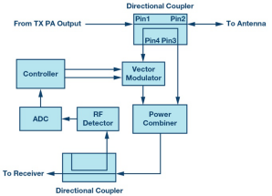
Figure 2. Typical Self-Interference Cancellation Circuit
Card reader key RF performance analysis
The block diagram of the SJC circuit including the RF front end of the UHF RFID reader is shown in Figure 3. ADI’s AD9963 integrates a dual-channel DAC and a dual-channel ADC. The ADF9010 integrates the transmitter modulator, PLL/VCO, receiver baseband filter, and PGA. The ADL5382 demodulator is included on the ADF9010 evaluation board. The ADL5523 is used as an LNA, which provides low noise figure, high gain, and high linearity. The 75 dB high dynamic range RF detector LT5538 is suitable for use with SJC RF power detectors.
For the transmitter, in the digital domain, the signal should be low-pass filtered to meet the ACLR requirements in the frequency domain, as well as the RF envelope requirements in the time domain. In the analog domain,

Figure 3. UHF RFID reader RF front-end block diagram.
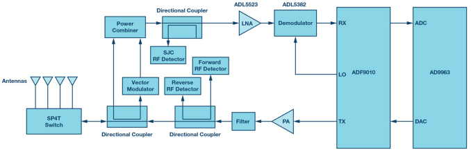
Figure 4. UHF RFID Reader RF Front End Using ADF9010 and AD9963
Both PA linearity and LO phase noise affect ACLR performance. After low-pass filtering, the peak-to-average ratio (PAR) of the ASK signal encoded by the TPP is about 2 dB. The average output power of the PA is about 32 dBm with a margin of 1 dB, so a PA greater than 35 dBm P-1 dB should be selected. For LO phase noise, the integrated phase noise should be less than -40 dBc from 125 kHz to 375 kHz and less than -60 dBc from 375 kHz to 625 kHz. For out-of-band emission requirements, an RF filter is required to meet the transmitter’s spurious requirements at harmonic frequencies. For requirements close to the operating frequency, e.g. at 915 MHz and 930 MHz, the noise requirement for a 100 kHz measurement bandwidth is C52 dBm, and the RF filter is generally not attenuated, so the noise floor requirement for the modulator at 0 dBm output power is approximately C52 C 10 × log10 (105) C 30 = C132 dBm/Hz. The phase noise requirement at 5 MHz offset should also be less than C132 dBc.
The sensitivity of the receiver is specified as -65 dBm in the GB/T 35786-2017 standard. Assuming the reader meets the -65 dBm sensitivity requirement at all possible data rates, a 640 kHz reverse link frequency (BLF) should be the worst case scenario. For an SJC containing an RFID reader, the insertion loss from the antenna port to the SJC output is about 15 dB, so the sensitivity requirement at the SJC output point is C80 dBm, assuming the tag backscattered signal power without DC is C80
C3 = C83dBm. The demodulation threshold of ASK modulated signal is about 11 dB, and the signal bandwidth of BLF 640 kHz uplink signal is 2.56 MHz. So the total NF requirement is: NF ≤ C83 C (C174 + 10 × log10 (2.56 × 10⁶) + 11) = 15.9 dB. This NF general requirement includes the noise impact of the receiver circuit after the SJC, the noise caused by the SJC circuit, and the transmitter leakage noise. Assuming that the delay between the signal branch of the vector modulator and the self-interference branch is matched, the SJC circuit can cancel the CW self-interference signal, and the leakage noise of the transmitter will also be well canceled. Transmitter leakage noise consists of three parts: phase noise, amplitude noise, and white noise. Typically, amplitude noise and white noise cancel to a noise floor of C174 dBm/Hz. For the remaining phase noise, since the transmitter and receiver use the same LO, it is converted to DC during downconversion due to distance-dependent effects. 6 In this case, the vector modulator branch noise will be the only additional introduced noise. Assuming the vector modulator branch noise floor is C162 dBm/Hz, so at the SJC circuit output, the effective NF is C174 C (C162) = 12 dB, then the NF requirement for the receiver circuit after SJC is 10 × log10 (101.59 C 101.2 ) = 13.6 dB.
ADF9010 and AD9963-Based Solutions
The ADF9010 is a fully integrated RF transmitter modulator, local oscillator (LO), and receiver analog baseband front end that operates from 840 MHz to 960 MHz. The AD9963 is a 12-bit low power MxFE® converter that provides two ADC channels sampling at 100 MSPS and two DAC channels sampling at 170 MSPS.
The block diagram of implementing the RF front end of a UHF RFID reader using the ADF9010 and AD9963 is shown in Figure 4. The cascaded NF of the ADL5523 with the ADL5382 and ADF9010 (receiver gain set to 24 dB) for the entire system is less than 3 dB.
In order to realize the RF front end of the UHF RFID reader, the author made two circuit boards. One is the SJC board including the adaptive SJC algorithm, and the other is the transceiver board integrating ADL5382, ADF9010 and AD9963. The two boards are cascaded together to test transmit and receive system-level RF performance.
For launch testing, a DSB-ASK encoded by TPP, 50% modulation depth, Tari set to a 12.5 μs RFID downlink waveform was constructed in Python® and downloaded to the FPGA board. Spectral domain ACLR and time domain RF envelope were tested on the antenna port with PA output power of 32 dBm. The test results are shown in Figure 5. For the ACLR test results, the adjacent channel values are approximately -42 dBc with a 2 dB margin, and the alternate channel values are -64 dBc with a 4 dB margin. For the RF envelope, the ripple is less than 1%, there is sufficient margin compared to the 5% limit, and the rise and fall times are both within the 1 μs and 8.25 μs limits.
For reception testing, a tag emulator was built using Analog Devices’ SPDT RF switch HMC545A, controlled by a microcontroller unit. The control mode is a list of RFID uplink FM0 encoded data. An ASK decoding program was constructed using MATLAB.®. By decoding the IQ using this program and comparing it to the raw data in the data list, the BER and receiver sensitivity can be calculated. Figure 6 shows the received IQ data and FFT plot. As can be seen from the figure, the program successfully decodes a -74 dBm RFID uplink signal with 320 kHz BLF.

Figure 5. Test setup diagram

Figure 6. Transmitter Test Results
Using the AD9361 to implement the front end
The AD9361 is a highly integrated radio frequency (RF) transceiver capable of various configurations for a wide variety of applications. It integrates all the RF, mixed-signal and digital blocks required to provide all transceiver functions in a single device. To implement a UHF RFID reader, the transmitter and receiver should use the same LO to take advantage of distance-dependent effects, so use the AD9361 transmitter to monitor the path instead of the regular receiver path. The AD9361 transmitter monitor path bypasses the internal LNA, so an external LNA, such as the Analog Devices ADL5523, is added. The ADL5523 is a high performance GaAs pHEMT LNA with 0.8 dB NF and 21.5 dB gain. The block diagram shown in Figure 8 shows the AD9361 used to implement the UHF RFID reader RF front end. This AD9361-based solution is significantly simplified compared to discrete component solutions. The AD9361 baseband is DC coupled, not AC coupled. In this case, the SJC circuit needs to be able to reduce the self-interference signal to a low enough level, for example, less than C35 dBm, to avoid saturation of the analog circuit. Therefore, the self-interference converted DC signal can be removed in the digital domain.
The AD9361 transmitter monitor path gain distribution consists of two parts of gain: the front end gain (transmitter monitor gain) and the receive low pass filter gain (GBBF). The transmitter monitor gain can be set to 0 dB, 6 dB or 9.5 dB. GBBF can be set from 0 dB to 24 dB in 1 dB steps. With this flexible gain configuration, receiver AGC functionality can be easily implemented. For this UHF RFID reader application, the transmitter monitoring path gain is set to 3 dB and the GBBF is set to 6 dB. The cascaded NF of the transmitter monitor port of the ADL5523 and AD9361 is approximately 12.6 dB when the AD9361 gain is set to 3 dB.This setup has a 1 dB margin compared to the 13.6 dB analysis requirement, if the residual self-interfering signal is
-35 dBm, the digital domain power is C7 dBfs.

Figure 7. Received receiver data FFT plot and decoded data

Figure 8. Block Diagram of UHF RFID Reader RF Front End Using AD9361

Figure 9. Test setup block diagram
AD9361 based solution, test setup and results
To implement the UHF RFID reader RF front end, the previously mentioned SJC board containing the adaptive SJC algorithm is cascaded with the AD9361 for testing transmitter and receiver system level RF performance. The test setup block diagram and connection diagrams are shown in Figure 9 and Figure 10.
The test results are shown in Figure 11. For the ACLR test results, the adjacent channel values are approximately -42 dBc with a 2 dB margin, and the alternate channel values are -61 dBc with a 1 dB margin. For the RF envelope, the ripple is less than 1%, meeting the 5% limit margin requirement. Rise and fall times are within the 1 μs and 8.25 μs limits.
For receiver testing, a list of RFID uplink FM0 encoded data was constructed and downloaded to the signal generator SMW200A, which was then configured to transmit DSB ASK signals using this data list. The IQ data received by AD9361 is stored in the FPGA board and extracted to the PC using the FTP tool. Use MATLAB to build an ASK decoding program. Using this program to decode the data and compare it to the original data in the data list, the BER and receiver sensitivity can be calculated. Figure 12 shows the FFT plot and decoded data of the MATLAB program. Test results show that the program successfully decodes a -65 dBm RFID uplink signal with 640 kHz BLF.

Figure 10. Test setup diagram
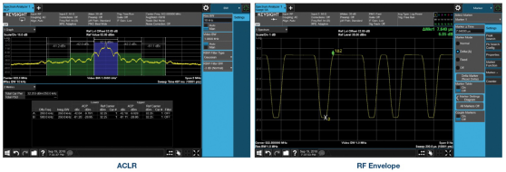
Figure 11. Transmitter Test Results Conclusion
This paper begins with an overview of China’s automotive electronic identification standards. It then analyzes the UHF RFID system-level link budget, key technologies employed in RFID (eg, SJC), and key RF performance requirements. Finally, set up the ADF9010 and AD9963-based solution, and the AD9361-based UHF RFID reader RF front-end for system-level performance testing. The solution based on ADF9010 and AD9963 has high performance and considerable margin, and can meet the requirements of GB/T 29768-2013 and GB/T 35786-2017. An integrated solution based on the AD9361 meets these requirements with reduced receiver sensitivity, which is significantly simpler than a discrete two-component approach. While the RF front-end described in this article is application-specific, the analysis methodology and the front-end itself are applicable to general UHF RFID reader solutions.

Figure 12. Received receiver data FFT plot and decoded data
references
1 GB/T 29768-2013 “Information Technology – Radio Frequency Identification – Air Interface Protocol (800/900 Mhz).”
2 GB/T 35786-2017 “General specification for reading and writing equipment for electronic identification of motor vehicles.”
3 Monza X Antenna Application Note. Impinj.
4 Gregor Lasser, Christoph F. Mecklenbrauker. “Self-Interference Noise Limits for RFID Readers.” 2015 IEEE International Conference on RFID, June 2015.
5 Alírio Boaventura, João Santos, Arnaldo Oliveira, Nuno Borges Carvalho. “Complete Isolation: Self-Interference Handling in Passive RFID Systems.” IEEE Microwave Journal, Vol. 17, No. 11, November 2016.
6 Byung-Jun Jang, Hyun-Goo Yoon. “Range-Dependent Effects of Phase Noise in UHF RFID Readers.” IEEE Microwave and Wireless Components Letters, January 2009
About the Author
Van Yang is Manager of Systems Applications Engineers at Analog Devices in Shanghai. Van joined ADI in 2015 as a Field Applications Engineer in Industrial and Medical Customer Support. Before joining ADI, Van worked at TI as a field applications engineer for over four years. He graduated from Huazhong University of Science and Technology with a master’s degree in Communication and Information Systems. Contact information:[email protected]


