

Content last revised on October 26, 2026
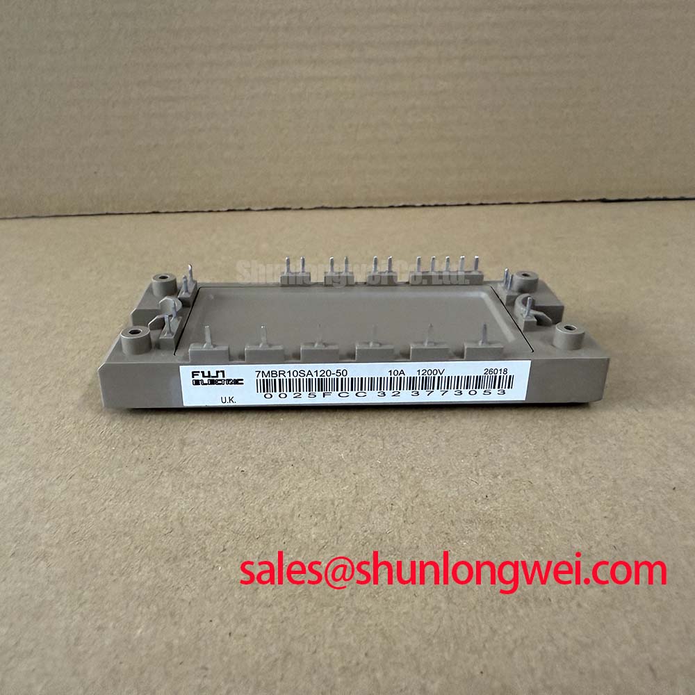
With the DC link discharged and its voltage checked, identify the power terminals of the 7MBR10SA120-50 against the equipment schematic before applying a multimeter in diode mode. Record probe polarity, isolate parallel circuit paths where practical, and compare corresponding conduction paths under the same cold conditions. A different reading deserves investigation, but a diode-mode result alone cannot establish switching performance, insulation integrity, or readiness for powered operation.
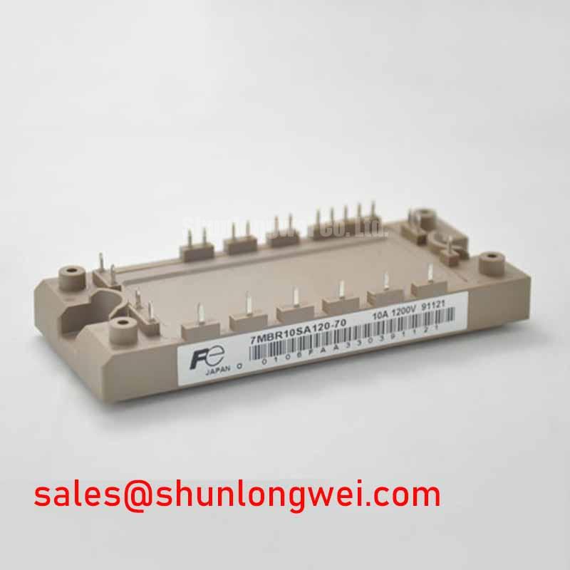
The Fuji Electric 7MBR10SA120-50 is a PIM power module with a 1200 V voltage rating, a 10 A current rating, and the package designation Fuji Power Module. These are the Official Specification values used here. Incoming inspection should keep the electrical rating check separate from the terminal-map and mechanical-fit checks, because each answers a different compatibility question.
💡 Bench Tip: Use ESD precautions and compare cold diode-mode readings with a known-good reference using the same meter, probe polarity, and terminal isolation. Record those conditions alongside the measurements so another technician can repeat the comparison without interpreting undocumented bench habits.
Benchtop Waveform Tuning: Mitigating Stress via Regenerative DC-Bus Voltage Surge Dissipation on 7MBR10SA120-50
Capture the DC-bus voltage during commanded deceleration before changing a braking resistor or adjusting a drive parameter. As a Design Consideration, distinguish the slower rise associated with regenerative energy from the brief overshoot associated with switching. These events can appear on the same trace, but they require different corrective work. Correlating bus voltage with the braking command and resistor current helps establish whether the energy-discharge path operates when the controller requests it.
Trace the braking circuit from the schematic and terminal diagram rather than assuming that the module designation establishes every internal connection. Identify the brake-switch terminals, resistor connection, control path, and any external switching stage. If the equipment uses an external braking IGBT, its ratings and driver behavior belong to that separate component assessment. The 1200 V and 10 A ratings of this module do not specify the pulse capability of every element in the braking circuit.
For resistor evaluation, the Engineering Recommendation is to examine the actual deceleration energy, repetition pattern, permitted resistor operating temperature, and brake-switch loading together. A resistance measurement checks continuity and cold resistance; it does not establish energy absorption capability. Inspect connections and protective devices, then compare the measured braking pulse with the resistor manufacturer's pulse-loading documentation. Resistor selection also needs to respect the minimum resistance permitted by the drive or braking stage.
When the bus rises despite a braking command, inspect the command timing, switch response, resistor-current path, and controller fault record. An absent current pulse may reflect an interrupted circuit, a disabled driver, or a control condition that has not been satisfied. A current pulse accompanied by continued bus rise calls for a different investigation: the braking demand, available dissipation, and deceleration profile may be mismatched. Neither observation identifies a single failed part without further checks.
Keep braking-current routing and resistor wiring consistent with the equipment layout. As a Design Consideration, clearance and creepage depend on working voltage, insulation arrangement, contamination conditions, and the applicable equipment standard. Resistor placement also affects nearby wiring and enclosure temperatures. Check these relationships against the original assembly arrangement instead of assigning a universal spacing or mounting distance to the module.
Repeated braking pulses require a thermal assessment that follows the load cycle. Where the relevant semiconductor transient thermal impedance curves are available, use their stated boundary conditions to relate pulse losses to junction-temperature rise. A case-temperature reading alone does not reveal the peak junction temperature during a short event. Check the thermal interface, heatsink condition, and cooling path before attributing temperature-related trips to the semiconductor.
In equipment compatibility work, designers may evaluate this module for light industrial automation drives or multi-joint robotic articulators, subject to electrical, mechanical, and control-interface matching. Such equipment can produce closely spaced acceleration and deceleration events. Record the actual motion sequence during evaluation so braking behavior is assessed against the machine's duty cycle rather than an isolated stop.
Benchtop Waveform Tuning: Mitigating Stress via Isolated DC-DC Power Supply Sizing for High-Voltage Gate Drives on 7MBR10SA120-50
Measure each isolated gate-drive supply relative to its own local reference while monitoring the associated gate-to-emitter waveform. As a Design Consideration, supply droop, reference movement, and signal-isolator disturbances must be distinguished because each can alter the observed gate signal. Use probes with suitable working-voltage and common-mode capability, and check whether the probing arrangement itself changes the waveform.
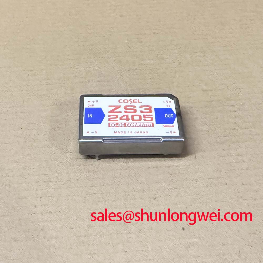
Size an isolated DC-DC supply from the selected driver's requirements, switching activity, gate-charge demand, and auxiliary loading. Its output voltage, regulation, startup behavior, and undervoltage response must match the drive circuit. Isolation test voltage and continuous working-voltage capability are different specifications. A reinforced-insulation claim requires supporting component documentation and an equipment-level insulation assessment; it cannot be inferred from a single withstand-voltage number.
The same distinction applies to common-mode transient immunity. CMTI characterizes the relevant isolator or driver under specified conditions, rather than establishing a universal requirement for this power module. The Engineering Recommendation is to compare the isolation component's documented performance with the common-mode transitions measured in the actual circuit. Check both signal polarities and operating states when investigating a gate disturbance that appears only during a neighboring switch transition.
For dead-time verification, observe complementary gate signals at the device connections and relate their timing to switching current. Controller timing alone omits propagation-delay differences, driver behavior, and device turn-off dynamics. Interlock evaluation should include startup, shutdown, undervoltage, and fault recovery. The required timing follows from the complete circuit's measured behavior across its intended operating conditions.
Desaturation protection also belongs to the driver assessment. As a Design Consideration, its sensing path, blanking behavior, threshold, and fault response must be coordinated with the transistor's documented short-circuit capability. Desaturation detection is distinct from measuring on-state collector-emitter voltage under controlled load. During fault evaluation, review the sensing waveform together with the gate discharge and collector-emitter voltage rather than judging protection from the fault-output signal alone.
A controlled soft turn-off can reduce the voltage excursion associated with interrupting fault current, but the shutdown profile must remain compatible with the device's short-circuit safe operating area. Avoid repeated deliberate fault events as a routine incoming-inspection method. Static checks establish a useful baseline; protection validation requires a controlled fixture, defined operating conditions, and the relevant device and driver limits.
The following comparison keeps the confirmed product ratings separate from the compatibility work required when considering another Fuji module. The 7MBR75VZ120-50 provides a related catalog reference for that evaluation, without establishing interchangeability.
| Comparison item | 7MBR10SA120-50 | 7MBR75VZ120-50 |
|---|---|---|
| Manufacturer | Fuji Electric | Fuji Electric |
| Voltage rating | 1200 V — Official Specification | Consult Datasheet |
| Current rating | 10 A — Official Specification | Consult Datasheet |
| Package designation | Fuji Power Module | Consult Datasheet |
| Replacement evaluation | Reference device for the equipment assessment | Compare terminal map, outline, drive requirements, protection, and thermal interface |
Fuji Electric's PIM 7-Pack product information supplies manufacturer context for the product category. Its separate power semiconductor and IPM resources help distinguish product families; a PIM classification alone does not establish integrated gate-drive or protection functionality.
Benchtop Waveform Tuning: Mitigating Stress via Turn-Off di/dt-Induced Vpeak Clamping on 7MBR10SA120-50
Measure collector-emitter voltage at the module connections during turn-off, with the voltage and current traces aligned closely enough to identify the associated transient. As a Design Consideration, probe-loop pickup and common-mode measurement error can exaggerate apparent ringing. Check measurement repeatability and probe placement before altering a gate resistor, snubber, or clamp.
An Engineering Calculation can estimate the inductive contribution using Vpeak ≈ VDC + Lsigma × |di/dt|, where Lsigma represents the effective commutation-loop stray inductance. This simplified relationship explains why loop geometry and current fall rate affect overshoot; diode recovery, capacitance, and ringing can also influence the measured peak. Compare the complete waveform with the 1200 V rating and the applicable switching limits when establishing the operating margin.
Reduce unnecessary commutation-loop area and examine the connection between the local DC-link capacitor and switching terminals. Closely coupled outgoing and return conductors can help reduce loop inductance. Symmetrical routing can also improve consistency between comparable paths, although mechanical symmetry alone does not prove equal electrical behavior. Final geometry should follow the equipment's insulation, assembly, and measured switching requirements.
Evaluate a snubber or clamp against the transient it must control. The Engineering Recommendation is to consider pulse current, repetitive energy, voltage stress, component heating, and connection inductance together. A capacitor value selected only to suppress visible ringing may transfer excessive loss elsewhere. Recheck the gate waveform and switching losses after a change, since a cleaner voltage trace does not by itself establish an acceptable operating point.
Trace adjacent power stages independently during schematic review. A component such as the 6MBI20GS-060 is relevant as a separate power-stage comparison, not evidence of a compatible rectifier or auxiliary-stage replacement. Confirm each stage's circuit function, voltage exposure, terminal arrangement, and control requirements before connecting its behavior to this module's transient stress.
For broader margin-assessment context, the Power Electronics Masterclass can support review of selection and system reliability considerations. On the bench, retain the operating conditions beside each waveform: bus voltage, load current, temperature condition, switching command, and probe arrangement. Those records make an overshoot comparison useful when checking a repaired assembly against a known-good configuration.
If the equipment includes a bidirectional battery converter, assess that stage's charge and discharge losses separately rather than extending this module's ratings to the complete converter. Thermal cycling depends on the actual temperature excursions and load sequence. After correcting a switching transient, repeat the relevant operating sequence and inspect the thermal response, gate behavior, and protection timing to confirm that the change remains acceptable throughout that sequence.